
Power Plane Eddy Current Attenuation and Stitching via Parasitics in High Speed Substrates
Stitching via arrays and eddy current losses damp cavity resonances to suppress power plane noise in high-speed substrates.
Stitching via arrays and eddy current losses damp cavity resonances to suppress power plane noise in high-speed substrates.
Substrate copper roughness exceeding skin depth dampens cavity quality factor by extending surface current paths, demanding 3D surface area profiling and incoming batch screening.

Selecting dielectric substrates requires balancing dissipation factor, glass weave uniformity, foil roughness, and panel yields to meet high-speed impedance targets.
Dynamic top-to-bottom spray pressure balancing and zonal CAM compensation eliminate conveyor puddle variations to hold tight high-frequency trace impedance.

Pairing mid-loss resins with HVLP copper cuts high-frequency trace attenuation by up to 38 percent without forcing transitions to expensive ultra-low-loss substrates.
Mitigate PCB cavity damping by replacing lossy nickel finishes with immersion silver and controlling surface roughness below single skin depth.
Modelling interfacial roughness on hydrophobic polyimide requires 3D Sdr metrics and Huray models to balance mmWave attenuation against peel strength limits.
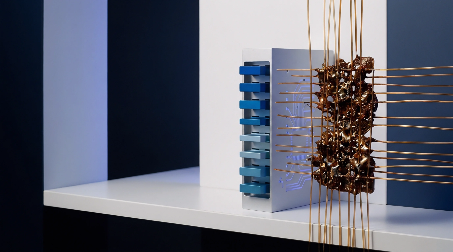
Inverting sub-terahertz dielectric tensors requires decoupling core micro-fracture damage from copper roughness spectral density to preserve phase velocity.

Resolving intermittent high speed signal integrity escapes requires pairing static boundary scan with embedded IJTAG at speed stress testing to catch dynamic physical layer failures.
Cyanate ester flexural stiffness induces adhesive shear lag and interfacial microcracking, causing rosette signal loss and latent solder interconnect escapes.
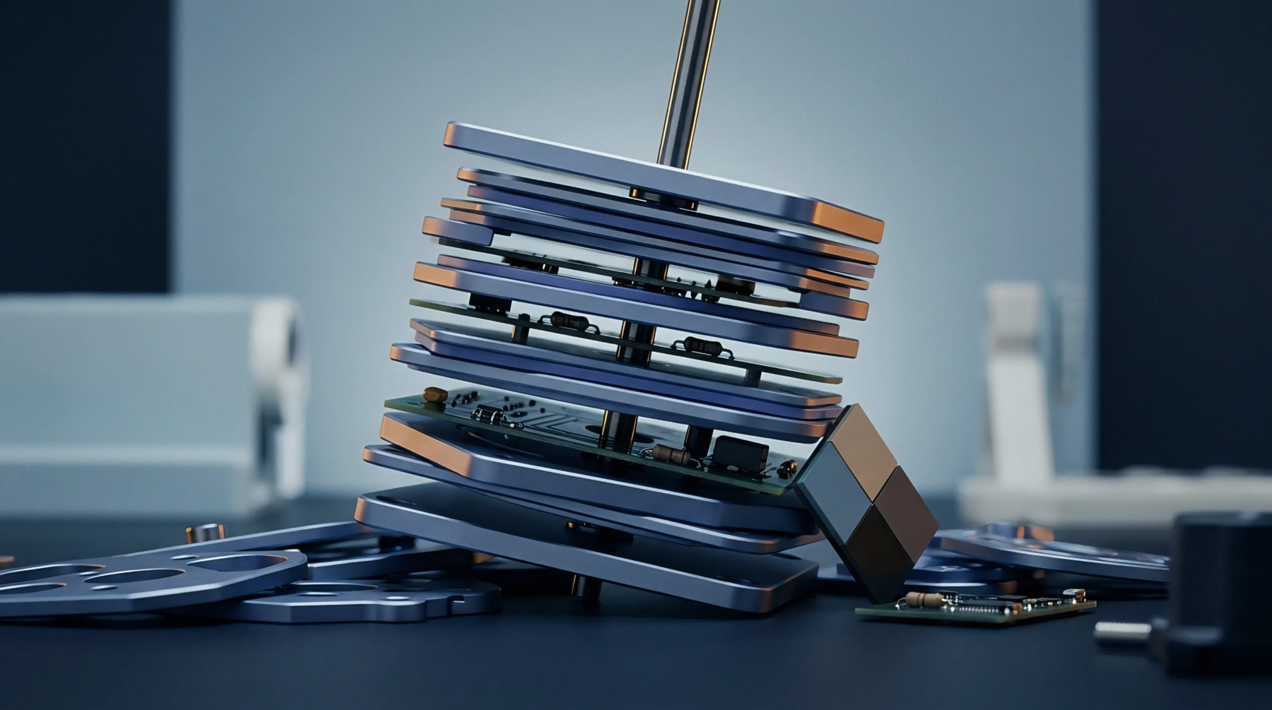
Quantifying aging micro-fractures in high-Q cavities links mechanical strain to Q-drop and out-of-band field escape spectra breaching EMC limits.

Dielectric characterization methods determine in-circuit signal velocity by accounting for test fixture field structure, glass anisotropy, and copper surface roughness.
Extrapolating high-temperature laminate loss tangent shifts prevents gigahertz plane edge emissions escapes caused by thermal cavity resonance shifts.
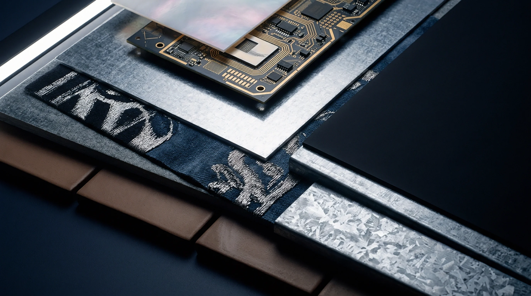
Quasi-optical extraction isolates intrinsic substrate loss from copper roughness, requiring explicit z-axis anisotropy conversion for accurate mmWave stackup design.
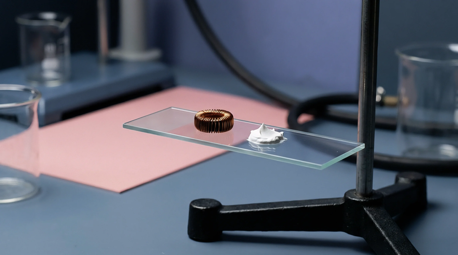
Decoupling tensor permittivity from interfacial scattering requires multiline TRL calibration and broadband power spectral density modeling up to 110 GHz.
Copper surface roughness increases high frequency cavity conductor attenuation by extending skin current path length and degrading unloaded quality factor.
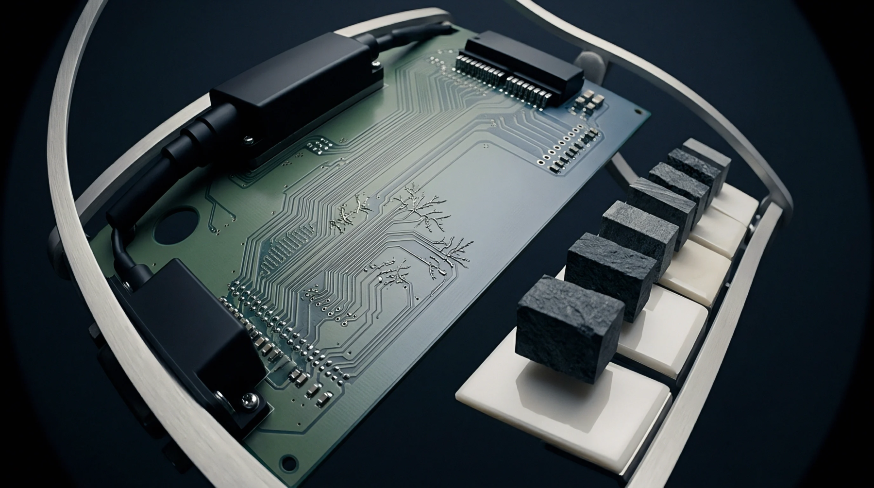
High-frequency phase delay anisotropy stems from woven reinforcement and foil grain directions; locking panel alignment ensures repeatable channel timing.
Boundary slip velocity models replace empirical roughness factors with electron specularity parameters, predicting insertion loss and phase delay up to 110 GHz.
Foil roughness forces skin currents through sub-micron surface teeth above 10 GHz, requiring Huray snowball modeling and low-etch oxide chemistries.
Etch factor quantification converts trapezoidal microstrip sidewall angles into accurate field solver inputs to prevent high-frequency impedance shifts.
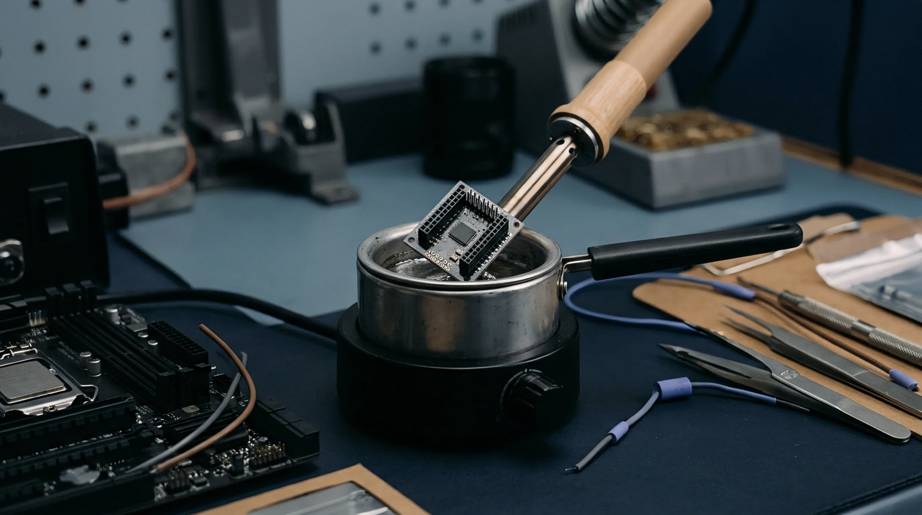
Modulating trace geometries against local interfacial dielectric gradients stabilizes phase velocity across millimeter wave interconnects.
Dielectric anisotropy in sub-THz glass substrates demands multi-mode resonant and transmission line metrology to decouple in-plane from out-of-plane permittivity.
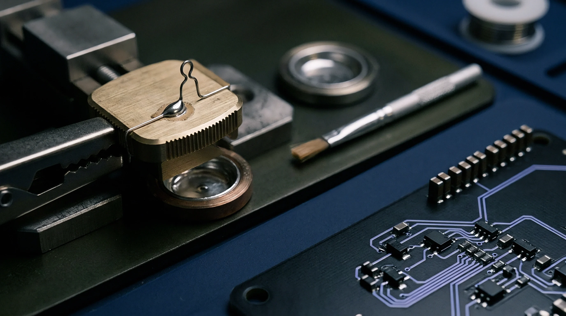
Fluoropolymer substrates absorb minimal water, but interfacial moisture traps degrade dielectric loss and shift high-frequency attenuation stability over time.
Formulate multi-frequency AC impedance guardbands by applying asymmetric root-sum-square budgets that absorb moisture uptake and vector de-embedding shifts.
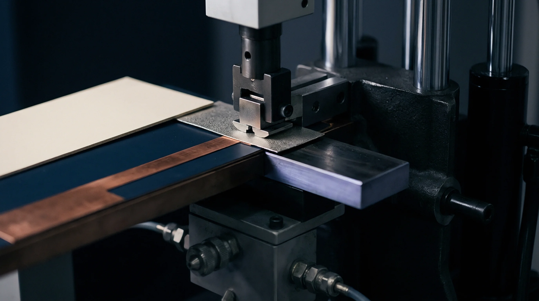
Analytical air gap de-embedding mathematically removes sample-to-fixture boundary voids to extract accurate substrate permittivity and prevent trace impedance scrap.

Match substrate TcDk and copper foil roughness on RF outer layers to cancel thermal phase velocity drift and maintain automotive radar target accuracy.
Differentiate foil roughness phase delay from glass weave skew by combining multiline TRL de-embedding with broadband phase-slope extractions on spread-glass coupons.
Sub-30 micron traces require 0.15 to 0.35 micron seed layers on ultra-smooth dielectrics, balancing high peel strength against rapid differential flash etching.
Environmental temperature and humidity cycling degrades substrate integrated waveguide cavity damping by elevating loss tangents and fracturing via fences.
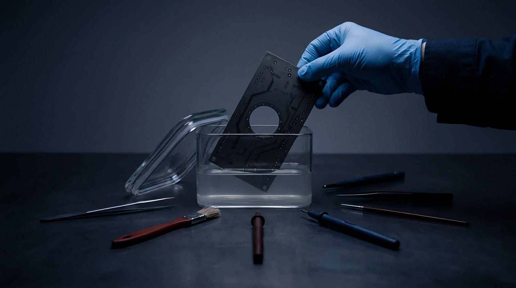
Characterizing printed losses requires isolating roughness skin depth from dielectric dipoles via de-embedded differential coupon extraction up to 50 GHz.
Expertise is a utility, not a secret. sentiention™ publishes its working knowledge as open reference: intelligence layer covering the materials it sources, the markets it enters, and the reference that serves both.