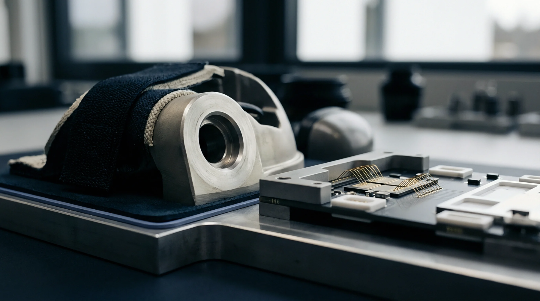
Substrate Integrated Waveguide Quality Factor Loss from Surface Profile Variations
Substrate profile roughness shrinks effective copper conductivity at millimeter-wave frequencies, degrading waveguide quality factor and increasing cavity loss.
Substrate profile roughness shrinks effective copper conductivity at millimeter-wave frequencies, degrading waveguide quality factor and increasing cavity loss.
Ground layer conductive losses at high frequencies depend primarily on copper foil surface roughness profiles and reference current loop paths.
Keep mesh pitch below twice the dielectric thickness at forty-five degrees to hold loop inductance within six percent of solid copper planes.

Phase distortion calibration extracts true propagation velocity by de-embedding fixture parasitics and compensating for copper profile inductance and weave skew.
High-frequency transmission line loss is minimized by selecting ultra-low-profile copper foils and spread glass laminates to limit roughness and phase skew.

High-speed differential lines require guard-banded TDR and VNA coupon testing to prevent localized trace defects from causing field failure escapes.
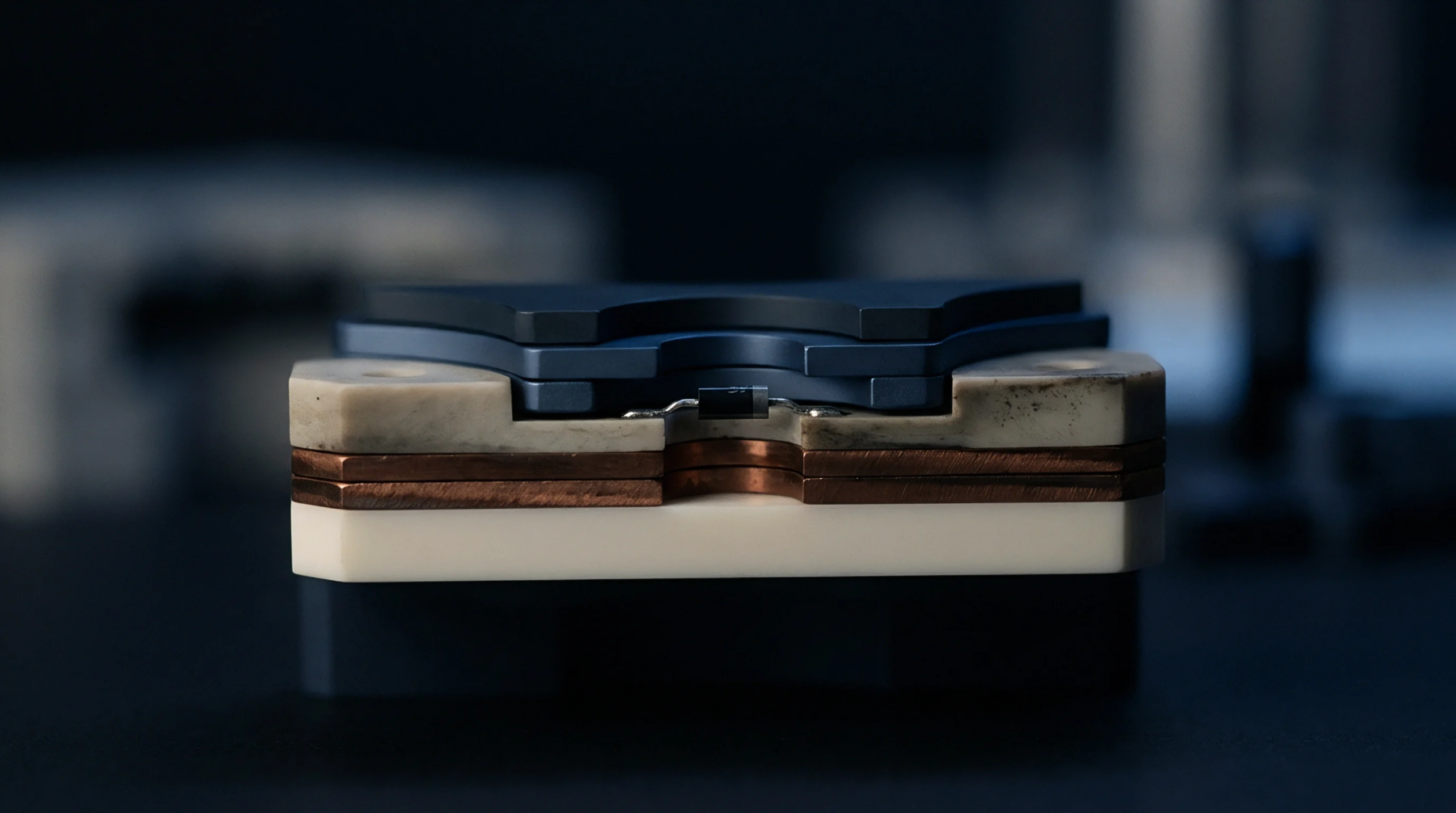
Sub-micron interfacial cracks trigger extreme local field enhancement and cold emission at high frequencies, demanding RF coupon testing over DC continuity checks.
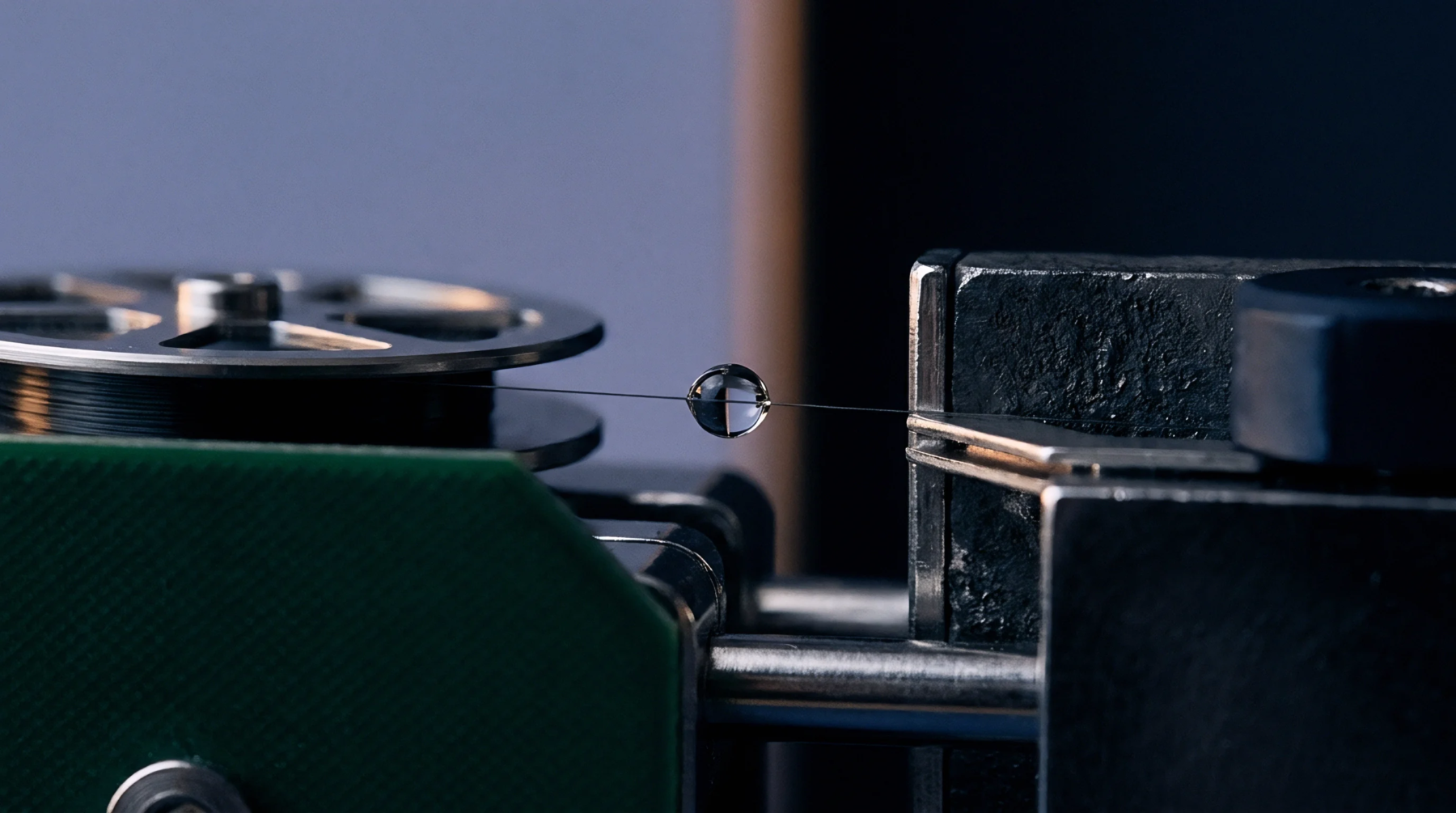
Target impedance modeling defines maximum power rail impedance limits across frequency to suppress transient voltage ripple through thin plane cavity stackups.

Calibrating HDI propagation delay demands de-embedding test fixture launches and extracting frequency-dependent permittivity from real coupon return geometries.
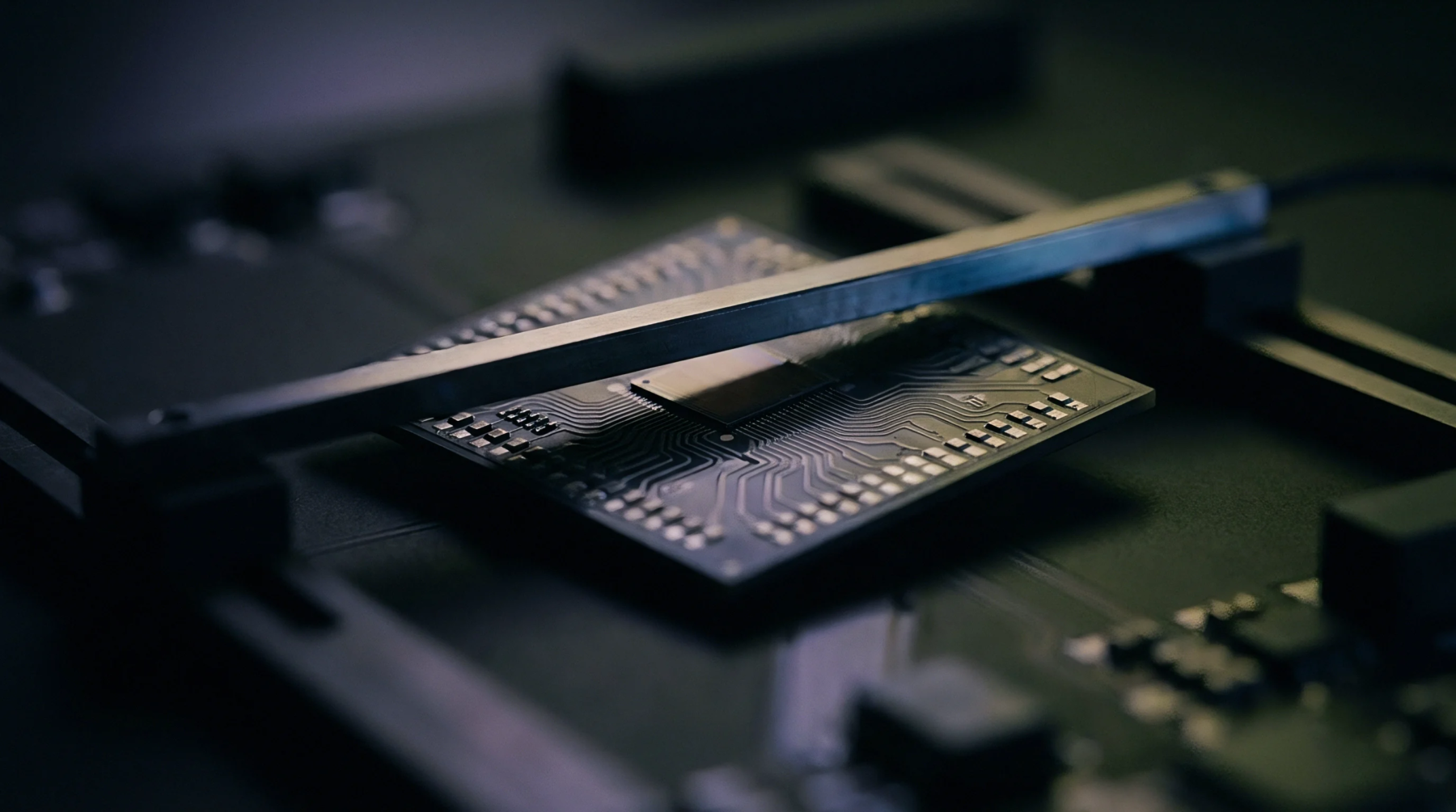
Extracting z-axis permittivity requires clamped stripline or disk resonators to isolate normal fields from in-plane glass weave bias and copper tooth delays.
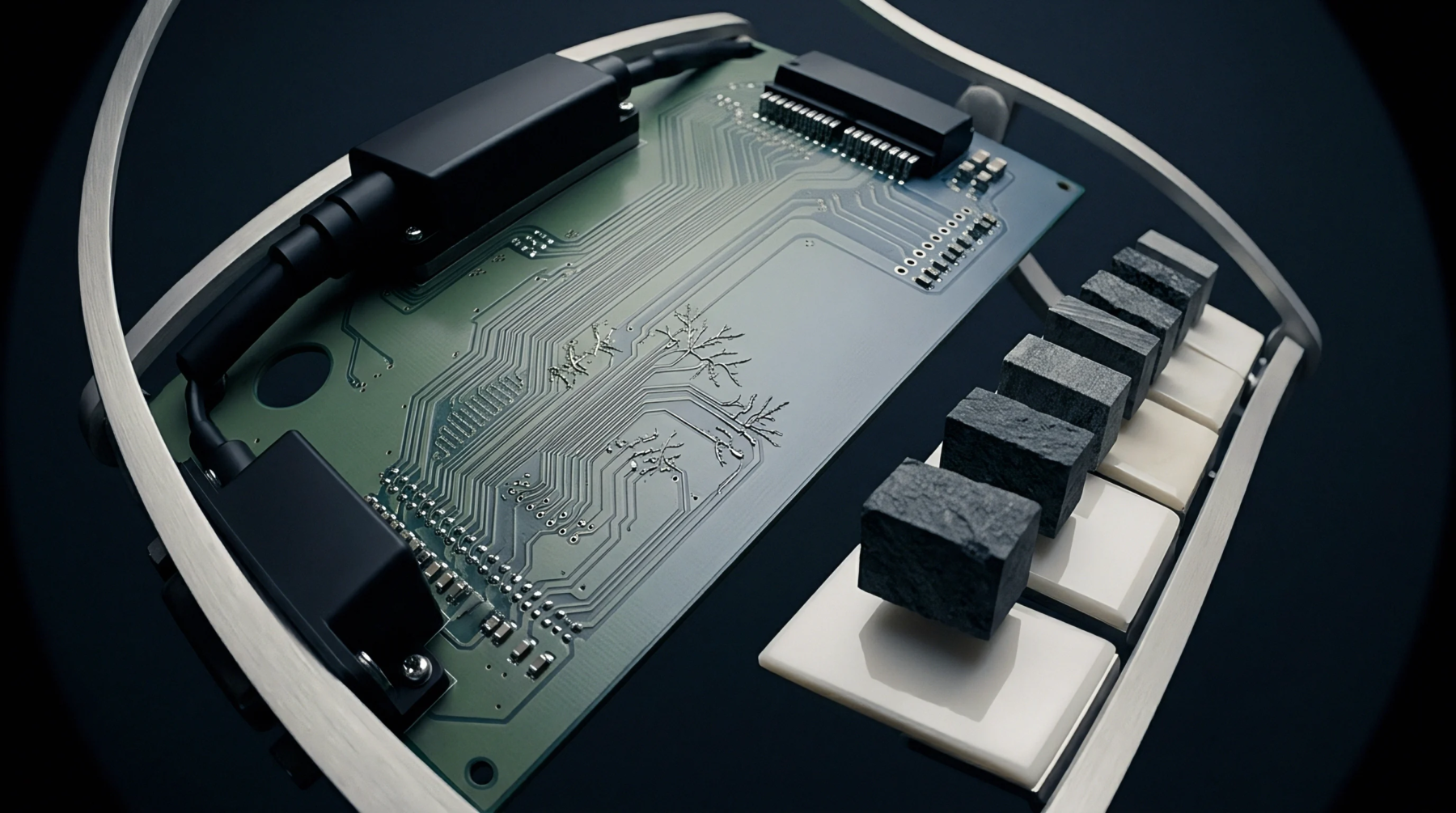
Nanoscale interface texturing eliminates target pad shear delamination in any-layer assemblies by swapping macro-mechanical teeth for molecular silane bonds.
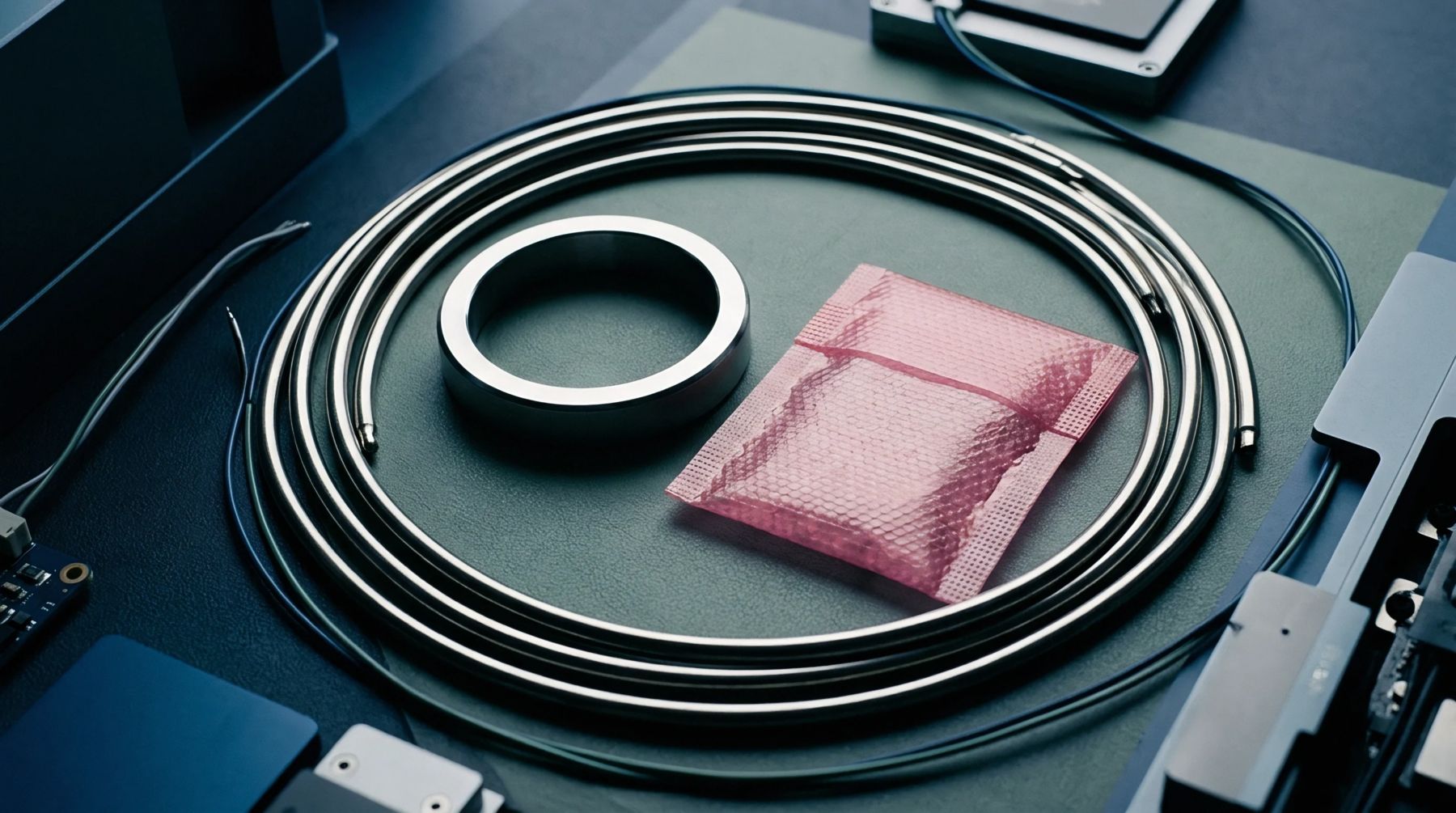
Deconvolving packaging core dispersion under humidity stress requires separating copper roughness from causal bound-water relaxation across anisotropic weave axes.
Sub-fifty-micrometre dielectric metrology requires edge fringing subtraction and Huray surface topography modeling to prevent massive impedance scrap.
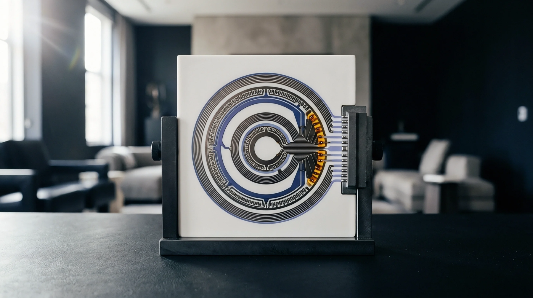
Fine pitch test socket insertion loss degrades through tin smear and plating wear, demanding cycle-based IEEE 370 de-embedding to prevent false scrap.

Sub-picosecond skew verification demands on-board planar TRL standards, mechanically spread glass weaves, and strict antipad probe relief geometry.
Anisotropic glass-resin matrices induce spatial permittivity shifts that degrade millimeter-wave phase velocity unless controlled by spread plies and foil choice.
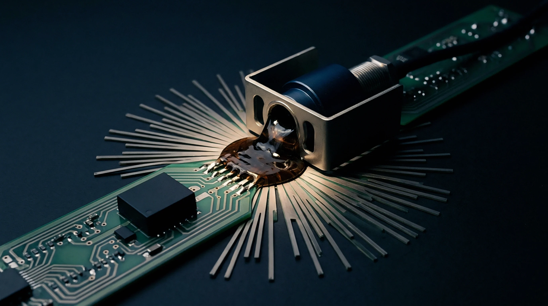
Operating thermal elevation shifts dielectric permittivity and expands layer spacing, driving gigahertz power plane edge radiation into non-compliance.

Extracting sub-terahertz dielectric tensors requires combining orthogonal transmission lines with multi-line TRL de-embedding to resolve anisotropic permittivity.
Atomic force power spectral density models sub-terahertz copper loss by mapping nanoscale spatial frequency harmonics that standard profile metrics ignore.
Etched sidewall taper concentrates high-frequency current into edge micro-roughness, doubling conductor losses above 50 GHz unless controlled by mSAP.

Etched PCB traces form trapezoids rather than rectangles; uncompensated sidewalls lower impedance by up to 4 ohms and amplify skin-effect losses above 10 GHz.
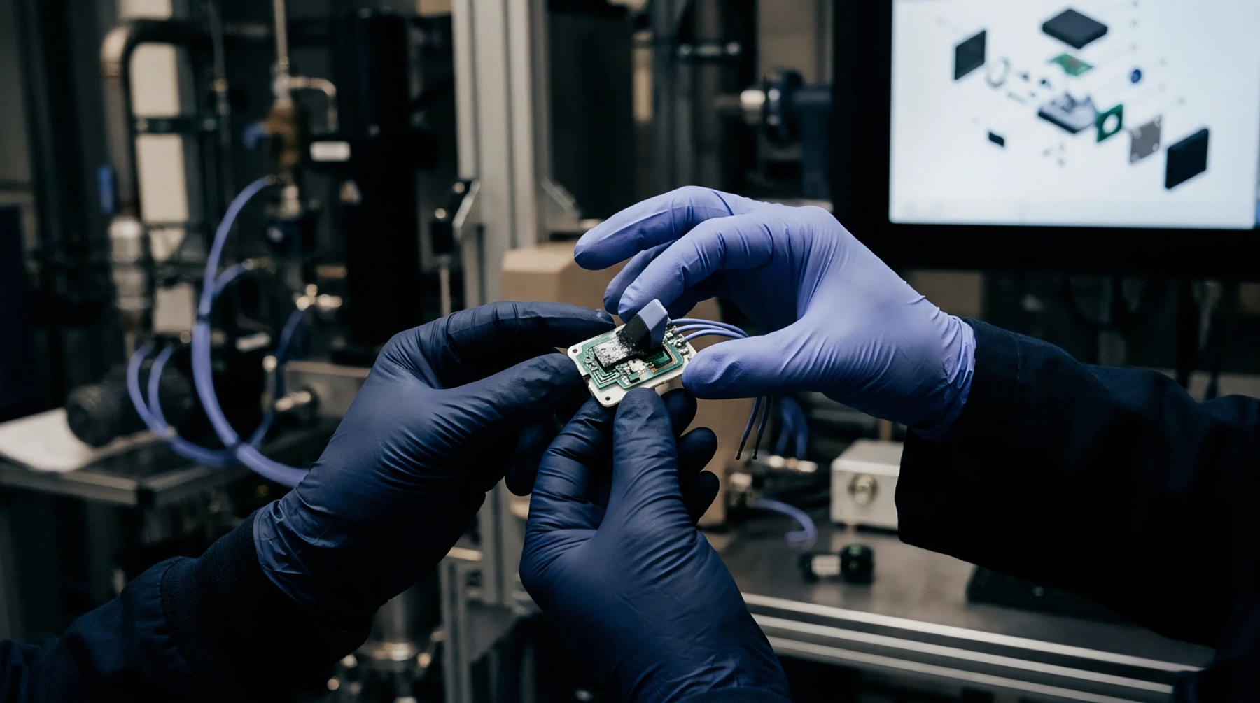
Predict long-term out-of-band field escape by modeling submicron plating fractures as dynamic slot radiators driven by thermal fatigue and harmonic currents.
Dynamic flexure drives interfacial tooth fracture and polymer relaxation, raising millimeter-wave attenuation long before DC resistance detects trace fatigue.
Low-profile copper foils reduce high-frequency conductor loss by minimizing surface roughness path extension, trading signal integrity against peel strength.

Reconciling coupon and quasi-optical permittivity requires de-embedding copper roughness phase delay and substrate tensor anisotropy from circuit measurements.

Predict sub-nanosecond common-mode coupling and parasitic shifts by modeling edge acceleration and extracting mixed-mode S-parameters before batch release.
Planar microvoids exceeding eight percent along solder perimeter boundaries trigger severe impedance mismatches, inducing high-frequency PAM4 eye diagram closure.
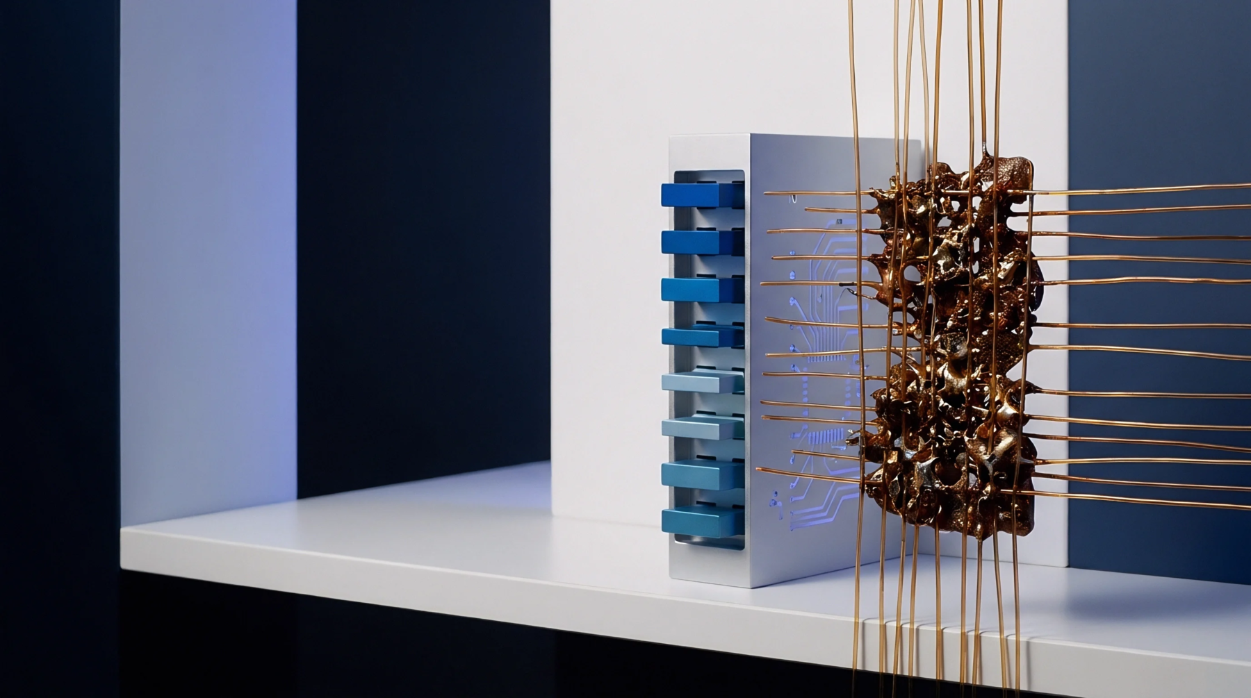
Aligning mid loss resin with very low profile foil minimizes high-frequency conductor loss while preventing peel strength failure during assembly.
Expertise is a utility, not a secret. sentiention™ publishes its working knowledge as open reference: intelligence layer covering the materials it sources, the markets it enters, and the reference that serves both.