
Controlling Transfer Efficiency across Stencil Apertures under Dynamic High Shear
Dynamic high shear drops solder paste transfer efficiency on sub-0.66 area ratios, demanding electropolished foils, controlled release, and strict SPI gates.
Dynamic high shear drops solder paste transfer efficiency on sub-0.66 area ratios, demanding electropolished foils, controlled release, and strict SPI gates.

Statistical process capability limits in surface mount lines require gauge R and R validation below ten percent before calculating paste volume and placement indices.

Stable liquid metal bearing hydrodynamic pressure keeps micro-focus X-ray focal spot jitter below 50 nanometers, preventing false void rejections in SMT inspection.

Active thermal management and real-time vector compensation eliminate focal spot movement to protect sub-micron solder joint inspection.

Proper test target placement ensures high structural fault coverage, prevents component damage, and reduces defect escapes in printed circuit assemblies.

Optimizing selective soldering nitrogen flow balances laminar oxygen displacement against gas turbulence, minimizing dross and defects at lowest landed cost.
Vertical solder rise quantification in plated through holes requires balancing pin-to-hole clearance, paste volume overprints, and thermal profile mass.

Reliable wave solder barrel fill depends on controlled radial gaps, complete flux activation, and thermal preheat profiles matching IPC Class 3 limits.

Embedded fiber optic sensors measure real-time gantry strain at five kilohertz, eliminating dynamic placement errors without throttling machine acceleration.

Matching solder paste flux mass loss derivatives to reflow profiles before alloy liquidus minimizes gas entrapment and eliminates bottom-terminated voiding.

Interleaving ground return pins within test fixture matrices reduces parasitic loop inductance, suppressing ground bounce jitter during high-speed functional testing.

Electroformed step-down stencils deliver tighter volume control than nano-coated steel below 0.50 area ratio, provided keepouts exceed 1.2 mm per 25 µm step.
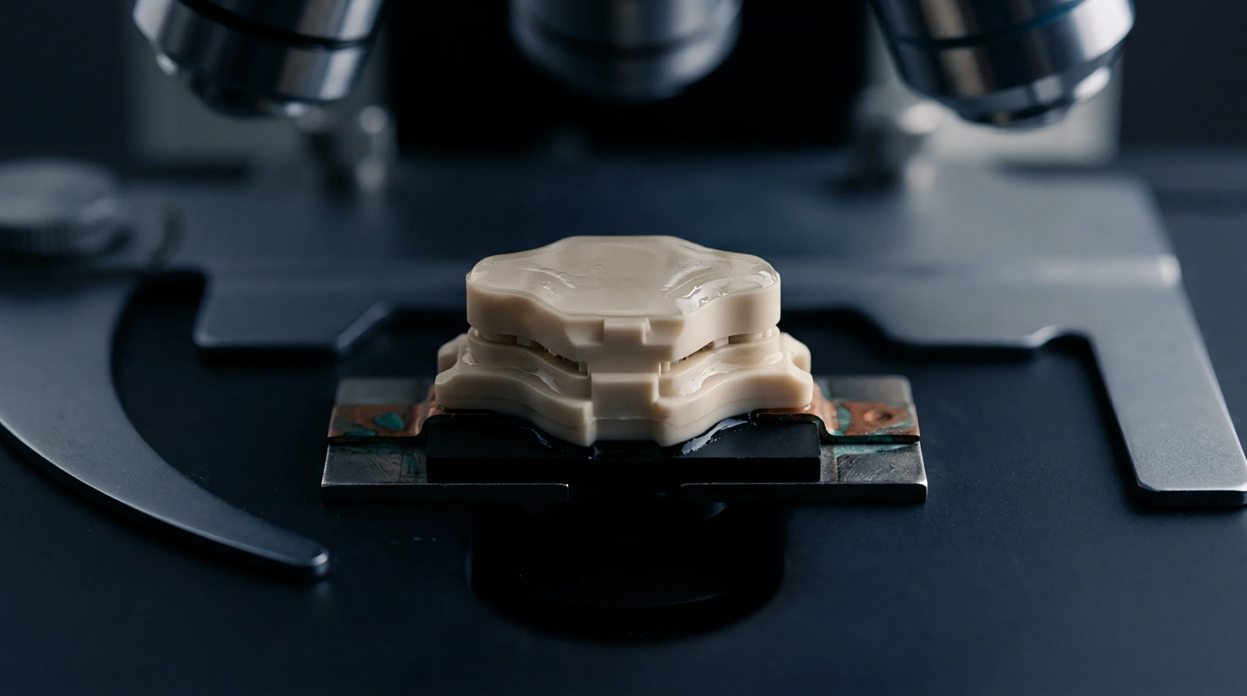
Establishing baseline stencil aperture ratios above 0.55 ensures consistent paste transfer efficiency and prevents post-reflow solder defects.

Continuous stencil shear reduces solder paste viscosity; maintaining print volume requires balancing squeegee speed, roll diameter, and paste turnover rates.
Parallel plate oscillatory strain sweeps validate high-speed deposit release by measuring storage modulus breakdown and yield stress thresholds.

Non-clean Type 4 paste recovery limits demand strict dwell caps to prevent cold slump and stencil clogging on fine-pitch assembly lines.
Incomplete physical test access increases latent structural defect escape rates, requiring complementary boundary scan and X-ray testing to protect field reliability.

IEEE 1149.6 boundary scan overcomes DC blocking in high speed differential pairs by evaluating edge transition pulses across embedded capacitive decoupling networks.

Hybrid regimes combine physical in-circuit probes for analog passives with IEEE 1149 boundary scan to close high-density BGA structural fault coverage gaps.
Calibrating piezoelectric z-axis hysteresis via closed-loop charge drive eliminates dynamic placement impact errors on continuous flex assembly lines.

Transfer efficiency below 0.66 area ratio hinges on paste yield stress and wall shear thinning, where oscillatory rheology separates printable lots from defects.
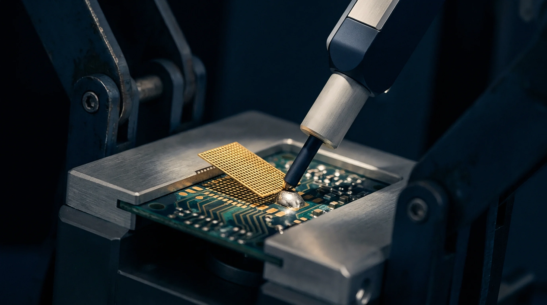
Sub-0.50 area ratio printing requires non-Gaussian statistical process control limits, Type 5 paste, and nano-coated stencils to prevent severe volume starvation.
Boundary scan testing uses a five-pin TAP interface and 16-state controller to verify PCB trace integrity and detect assembly faults without physical probe access.

Nano coated stencils sustain solder paste transfer efficiency above seventy-five percent across sub point six area ratios by reducing aperture wall friction.
Expertise is a utility, not a secret. sentiention™ publishes its working knowledge as open reference: intelligence layer covering the materials it sources, the markets it enters, and the reference that serves both.