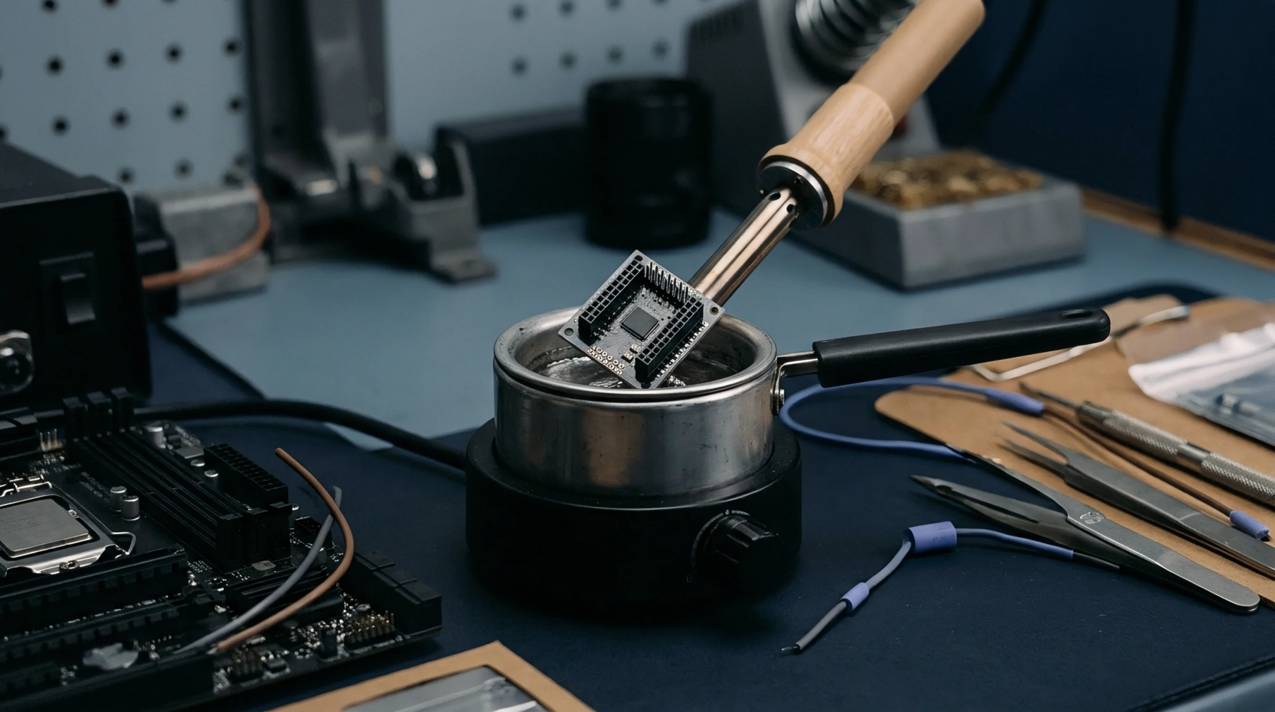
Failure Analysis Diagnostic Labor Allocation in Volume PCBA Rework Cycles
Diagnostic labor caps balance technician hourly payroll against scrap value to prevent unprofitable rework cycles on defective printed circuit board assemblies.
Diagnostic labor caps balance technician hourly payroll against scrap value to prevent unprofitable rework cycles on defective printed circuit board assemblies.
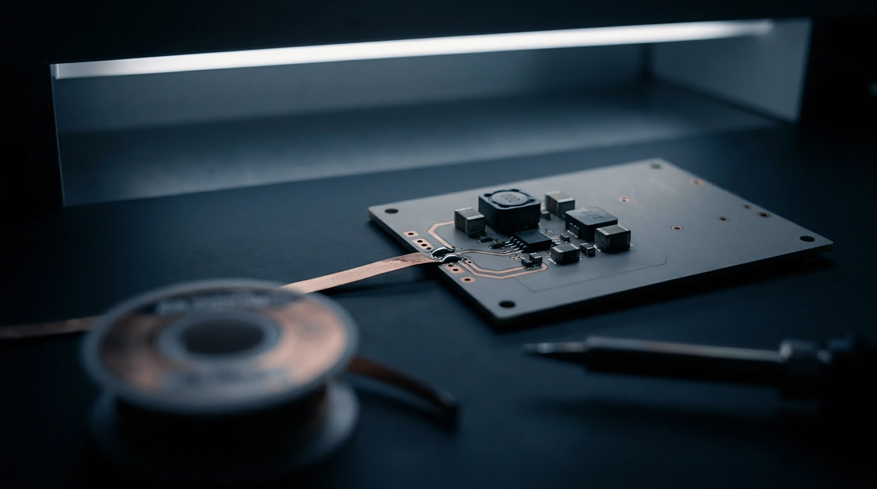
Adjusted first pass yield masks manufacturing defects and latent thermal damage through unlogged re-probes, widened guard bands, and hidden manual rework.
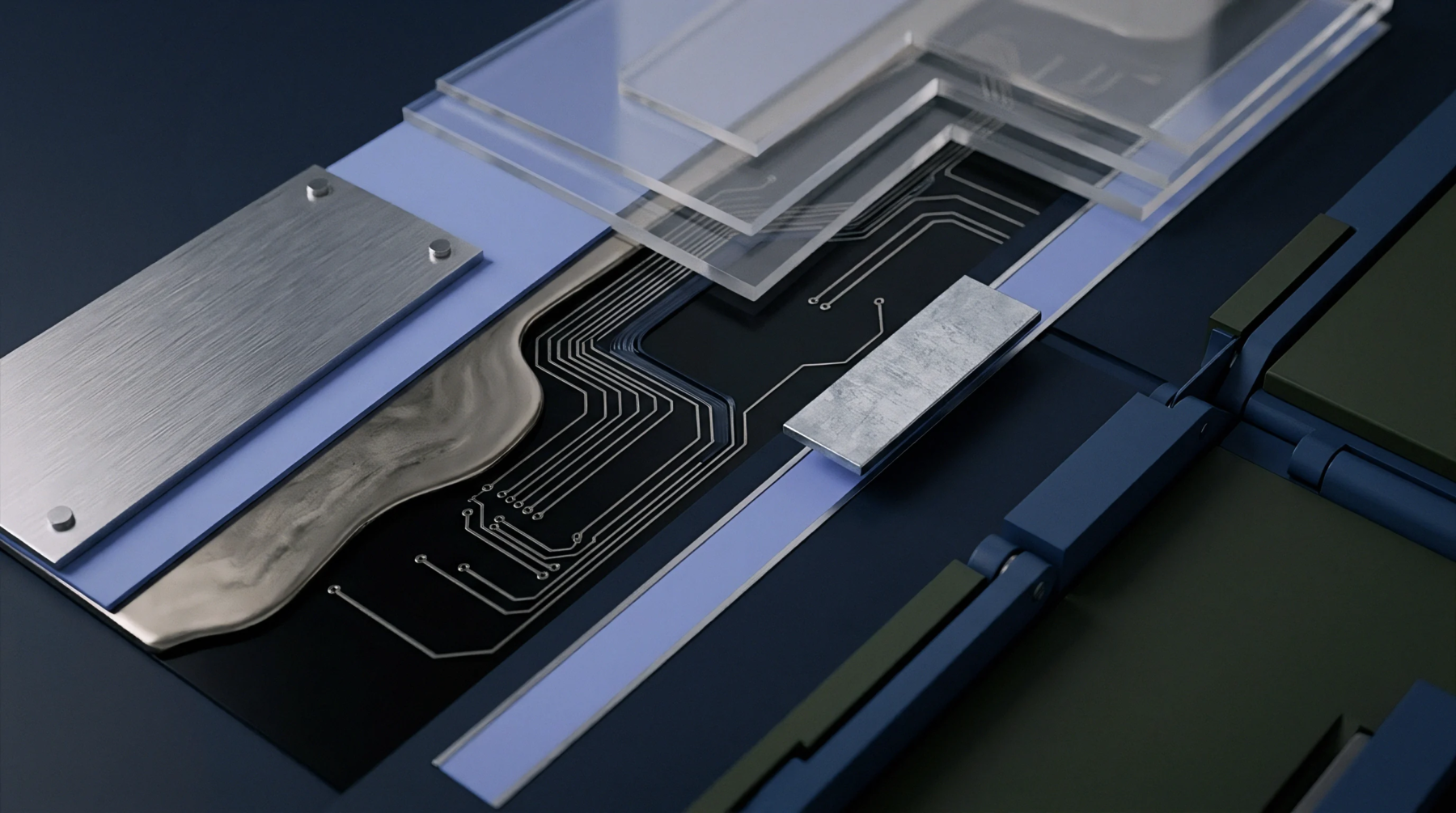
Verify 180-degree acoustic phase inversion at package interfaces post-bake to reject sub-micron delaminations before high-temperature reflow cracking occurs.

Thermal baking consumes fusible tin through solid-state intermetallic growth, limiting desiccation cycles before wetting failure halts high-speed placement lines.

Field return rates equal total screening escape rates scaled by operational duty cycle and environmental defect manifestation factors over time.
Dynamic reflow profiling and tailored carrier tooling compress panel thermal deltas below eight degrees Celsius, preventing joint defects on dense boards.

Fixture mechanics prevent board damage by holding strain below five hundred microstrain and enforcing forty-mil minimum test point pad spacing.
Sub-200 micron stencil release depends on paste extensional viscosity and wall slip, where nano-coatings reduce breakup time to ensure high transfer efficiency.
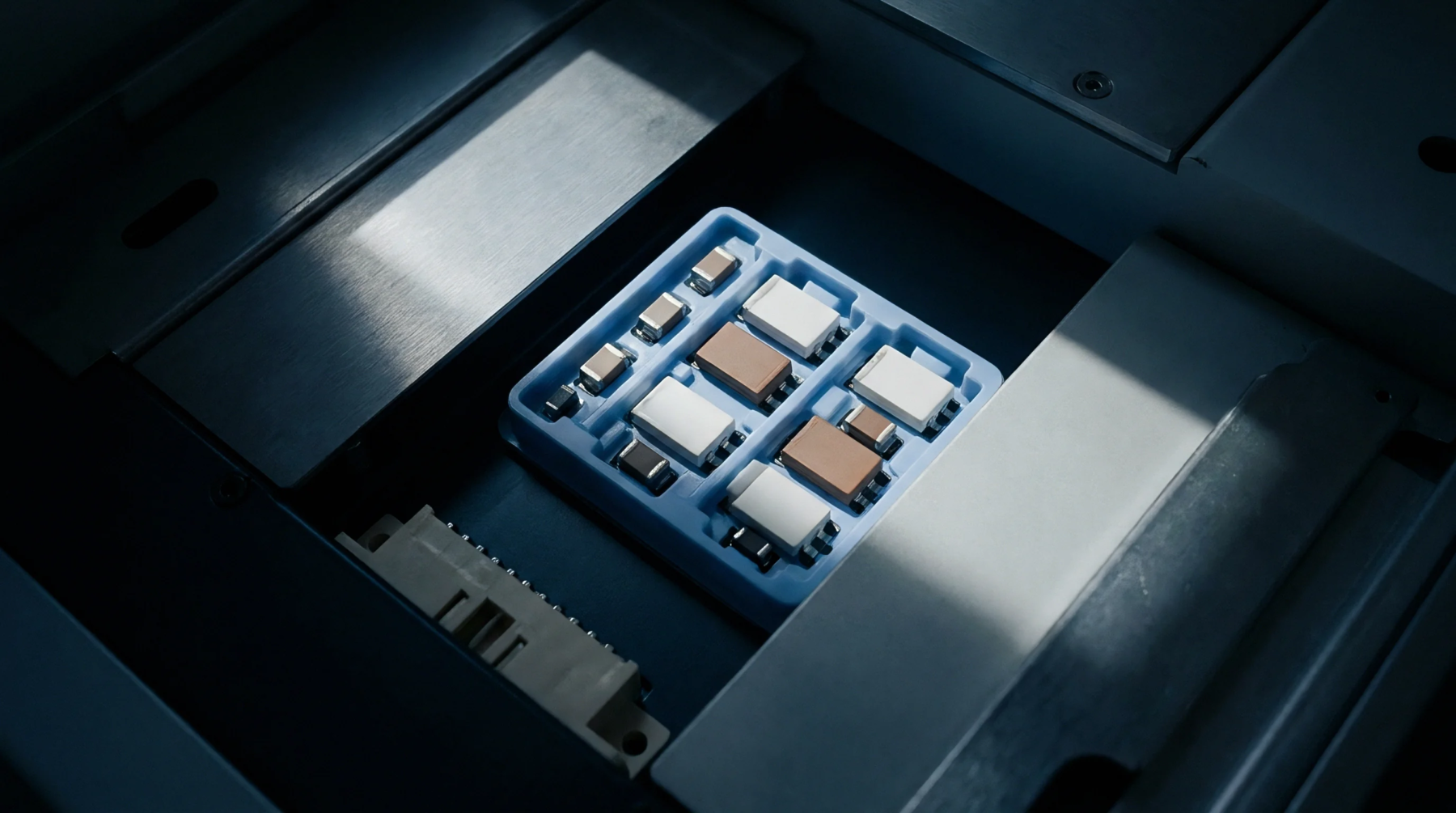
Controlled preheat soaking between 130°C and 160°C suppresses matrix hydrolysis by volatilizing absorbed moisture before organic acid activators dissociate.
Rigorous verification of PCBA artwork, BOM netlists, and compliance dossiers before release prevents receiving holds, line downtime, and field returns.

Dynamic multi-sensor thermal stage compensation maintains sub-micron inspection accuracy, preventing false solder joint defect calls on advanced packaging lines.
Real-time shadow moiré reflow integration monitors dynamic component warpage to modulate upper and lower furnace convection, preventing solder open defects.

Sub-0.5 area ratios starve solder volume, accelerating brittle intermetallic boundary defects that require stepped stencils and Type 5 paste to resolve.
Contractual labor chargebacks allocate false call review costs when automated optical inspection pseudo-defects breach agreed parts-per-million thresholds.

Production lines run stable when automated inspection yields fifty false calls per million solder joints without suppressing defect classification algorithms.
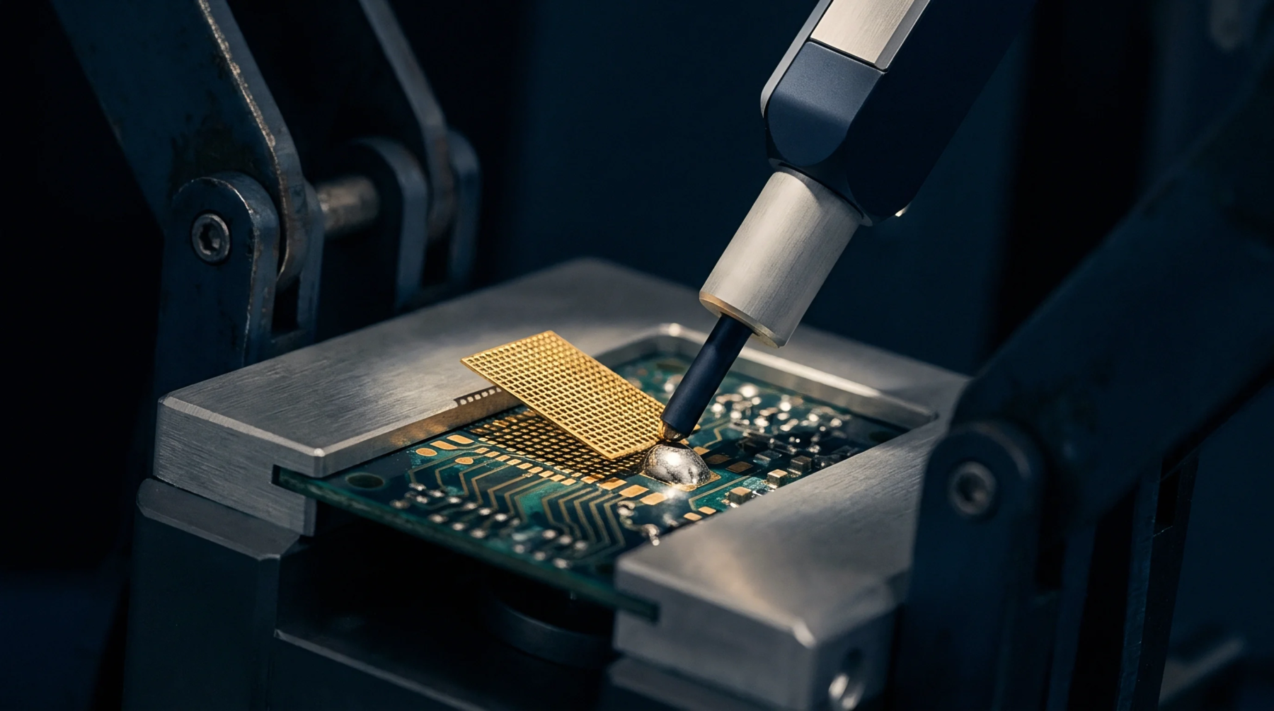
Optimizing reflow profiles requires balancing soak duration and cooling rates to minimize voiding, warpage, and brittle intermetallic growth.

Optimizing boundary scan access for high-density interconnects replaces physical probes with silicon registers, maximizing fault coverage and lowering test cost.
Flying probe capacitance screening locates open nets rapidly, while four-wire Kelvin micro-ohm verification isolates hidden trace necking and micro-via cracks.

Combined boundary scan and bed-of-nails access modeling calculates structural escape rates to prevent latent defect exposure in field shipments.

Non-redundant aggregation of optical, X-ray, and boundary scan coverage metrics determines true defect escape risk on high-density circuit boards.

Derating tactical placement speed protects actual assembly yield by suppressing kinetic vibration, feeder mispicks, and reflow defects before scrap costs accumulate.
Unified PCOLA-SOPS deduplication calculates combined structural coverage through strict Boolean fault-class scoring rather than naive additive percentages.

Contractual recovery for intermittent SMT failures requires 3D SPI volume logs, dynamic thermal profiles, and certified SEM intermetallic microsections.
SMT liabilities partition through synchronized SPI, AOI and feeder logs, setting attrition caps by package size and billing overages above contract baselines.
Unified test coverage requires de-duplicating shared fault opportunities across in-circuit probing and boundary scan using standardized PCOLA-SOQ metrics.

Solder paste deposit volumetrics directly dictate micro pitch SMT defect rates, requiring strict area ratio controls and 3D inspection limits to prevent bridging.

Isothermal solvent evaporation determination defines paste stencil life, rheological stability, and defect limits by tracking flux carrier loss over time.
Matching reflow soak durations to flux solvent evaporation rates eliminates sub-component pressure spikes and drops QFN thermal pad voiding below ten percent.
Electroformed stencil transfer efficiency drops under high speed printing due to binder separation and wall compaction, requiring optimized wipe cycles.

Micro-aperture solder paste transfer efficiency demands electroformed or nanocoated stencils, Type 5 powder, and strict 3D inspection controls below 0.55 area ratios.
Expertise is a utility, not a secret. sentiention™ publishes its working knowledge as open reference: intelligence layer covering the materials it sources, the markets it enters, and the reference that serves both.