Copper Budget
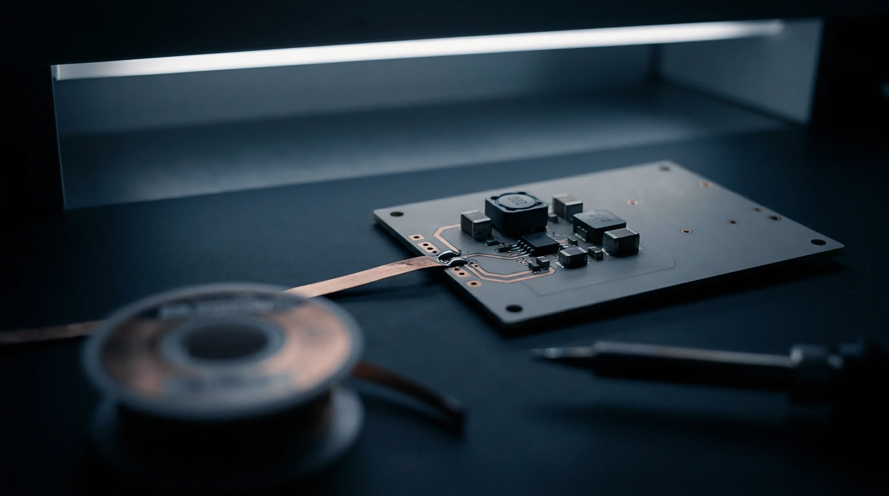
Surface mount technology routing requires exact spatial limits between printed circuit traces and adjacent lands to prevent solder bridging during reflow. Target pad separation establishes the minimum geometric clearance from a terminal land edge to the nearest copper feature, protecting against electrical shorts caused by excess paste volume. Photolithography mask registration errors during outer layer imaging can reduce this manufactured gap below safe thresholds.
Automated optical inspection equipment measures the resulting copper distance before solder paste deposition to flag etch anomalies. Minimum electrical clearance standards dictate that smaller spacing demands tighter solder mask dam dimensions on high density interconnect substrates.
Solder Mask
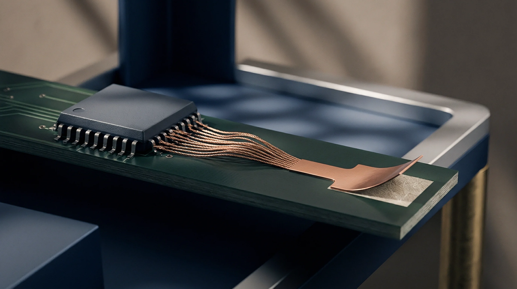
Liquid photoimageable lacquer acts as a physical barrier between adjacent metallic features on a printed circuit board. Target pad separation defines the required web width of this polymer coating residing between adjacent component lands. Insufficient resin thickness in the interpad channel permits liquid solder to bridge opposing terminals during thermal excursions.
Solder mask bleed onto component lands reduces the effective wetting area and creates weak intermetallic bonds.
Reflow Profile
Thermal convection ovens melt applied paste alloys to form permanent mechanical and electrical joints. Target pad separation influences thermal absorption rates across densely populated areas because nearby copper masses draw heat unevenly. Slow preheat ramps allow volatile solvents to escape before the flux system activates, preventing solder ball formation across narrow surface gaps.
Peak temperature zones must maintain uniform profiles to ensure complete wetting without bridging adjacent terminals.