
Boundary Scan Coverage and the Faults It Never Reaches
Boundary scan isolates structural opens and shorts on compliant nets, requiring hybrid physical probe testing to catch unmapped passives and dynamic failures.
Boundary scan isolates structural opens and shorts on compliant nets, requiring hybrid physical probe testing to catch unmapped passives and dynamic failures.
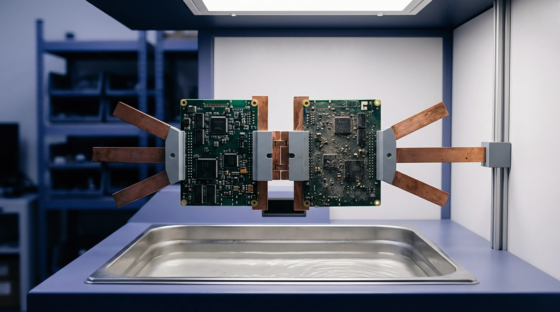
Boundary scan interconnect testing turns silicon multiplexers into virtual probes to verify fine-pitch BGA solder joints without physical test pads.

Boundary scan netlist coverage is bounded by physical TAP access, requiring explicit fault universe math to quantify unverified structural escape risks.

Integrating hybrid boundary scan and flying probe regimes eliminates unreached structural defects by establishing 99 percent nodal fault coverage.
Modeling probe parasitics and edge skew on boundary scan nets prevents false test failures and maintains scan chain timing margins under fixture actuation.

Boundary scan access limits require balancing physical probe suppression against quantitative fault escape risks in high-density logic clusters.
Deriving boundary scan coverage for high-density ASIC arrays requires precise accounting of scannable versus un-scannable nets to prevent costly field escapes.

Boundary scan TAP probe evaluation demands dynamic contact resistance monitoring under 20mV dry-circuit limits to prevent false structural defect calls.

Integrating IEEE 1149.1 boundary scan with flying probe target vectors maximizes fault coverage on high-density PCBs while slashing test times and fixture costs.

IEEE 1149 boundary scan delivers direct structural fault coverage on dense BGAs without physical probes by shifting test vectors through standardized internal chip logic.

Resolving boundary scan escape rates requires weighting fault coverage by defect universe and enforcing active guarding on unprobed parallel nets.

Quantifying boundary scan interconnect fault coverage pairs extracted netlist node universes with modified counting sequence vector execution logs.
Boundary scan integration replaces physical test points with silicon registers, securing structural fault coverage on high density circuit assemblies.

Integrating boundary scan vectors into bed of nails fixtures closes non-access coverage gaps while reducing physical probe strain and assembly rework costs.
Unified test coverage requires de-duplicating shared fault opportunities across in-circuit probing and boundary scan using standardized PCOLA-SOQ metrics.

Non-redundant aggregation of optical, X-ray, and boundary scan coverage metrics determines true defect escape risk on high-density circuit boards.

Boundary scan replaces physical fixture probes by shifting serial test patterns through dedicated on-chip registers to prove high-density ASIC solder integrity.
Combined boundary scan and bed-of-nails access modeling calculates structural escape rates to prevent latent defect exposure in field shipments.
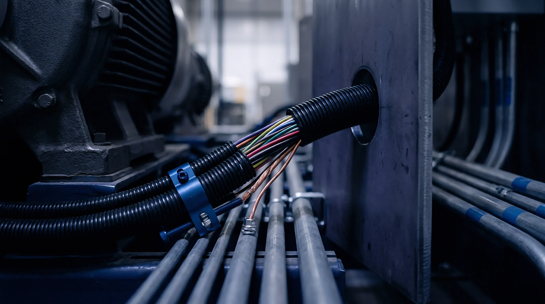
Physical TAP probe contact mechanics dictate constriction resistance, where inadequate normal force and oxide films corrupt boundary scan signal integrity.

Dynamic TAP contact resistance drift attenuates boundary scan signals, causing structural fault escapes that violate product conformity declarations.

Optimizing boundary scan access for high-density interconnects replaces physical probes with silicon registers, maximizing fault coverage and lowering test cost.

Hardware triggers synchronizing probe tip mechanical settling with JTAG vectors eliminate false opens and bus contention on high-density circuit assemblies.

Boundary scan accessibility delivers over 95 percent structural interconnect coverage on high-density assemblies without physical bed-of-nails test probes.
Configure clean TAP terminations, verify BSDL instruction registers, and execute EXTEST vectors to isolate physical solder bridges and open joints.
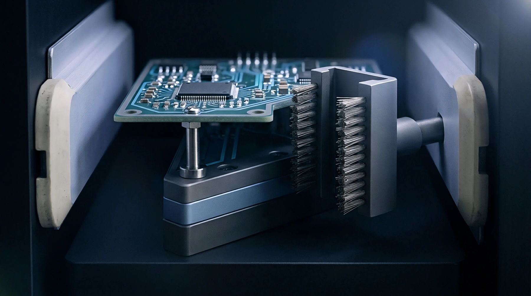
Integrating boundary scan files into in-circuit fixtures reclaims blind BGA net coverage, cuts mechanical probe force, and lowers board diagnostic debug costs.
Managing test access loss requires combining miniature spring probes, boundary scan, and 3D X-ray inspection to prevent expensive latent defect field escapes.
Embedded IJTAG PRBS instruments run during stress screening capture transient interconnect failures that static functional bench tests miss.
Structural coverage on unprobed HDI boards requires weighted PCOLA-SOST defect modeling combining IEEE 1149.6 AC scan, 3D X-ray slice data, and optical vision matrices.

Boundary scan testing uses a five-pin TAP interface and 16-state controller to verify PCB trace integrity and detect assembly faults without physical probe access.

Boundary scan cell allocation dictates structural fault coverage by converting physical IC pins into software-driven stimulus and response registers.
Expertise is a utility, not a secret. sentiention™ publishes its working knowledge as open reference: intelligence layer covering the materials it sources, the markets it enters, and the reference that serves both.