
Electrical Test Coverage Metrics in Printed Circuit Assembly
Electrical test coverage metrics require mapping physical nodal access and test regimes against a complete structural fault universe to limit field escapes.
Electrical test coverage metrics require mapping physical nodal access and test regimes against a complete structural fault universe to limit field escapes.

First pass yield gaps in high-density assemblies stem from optical test blind spots, microvia structural fatigue, and restricted physical probe access.
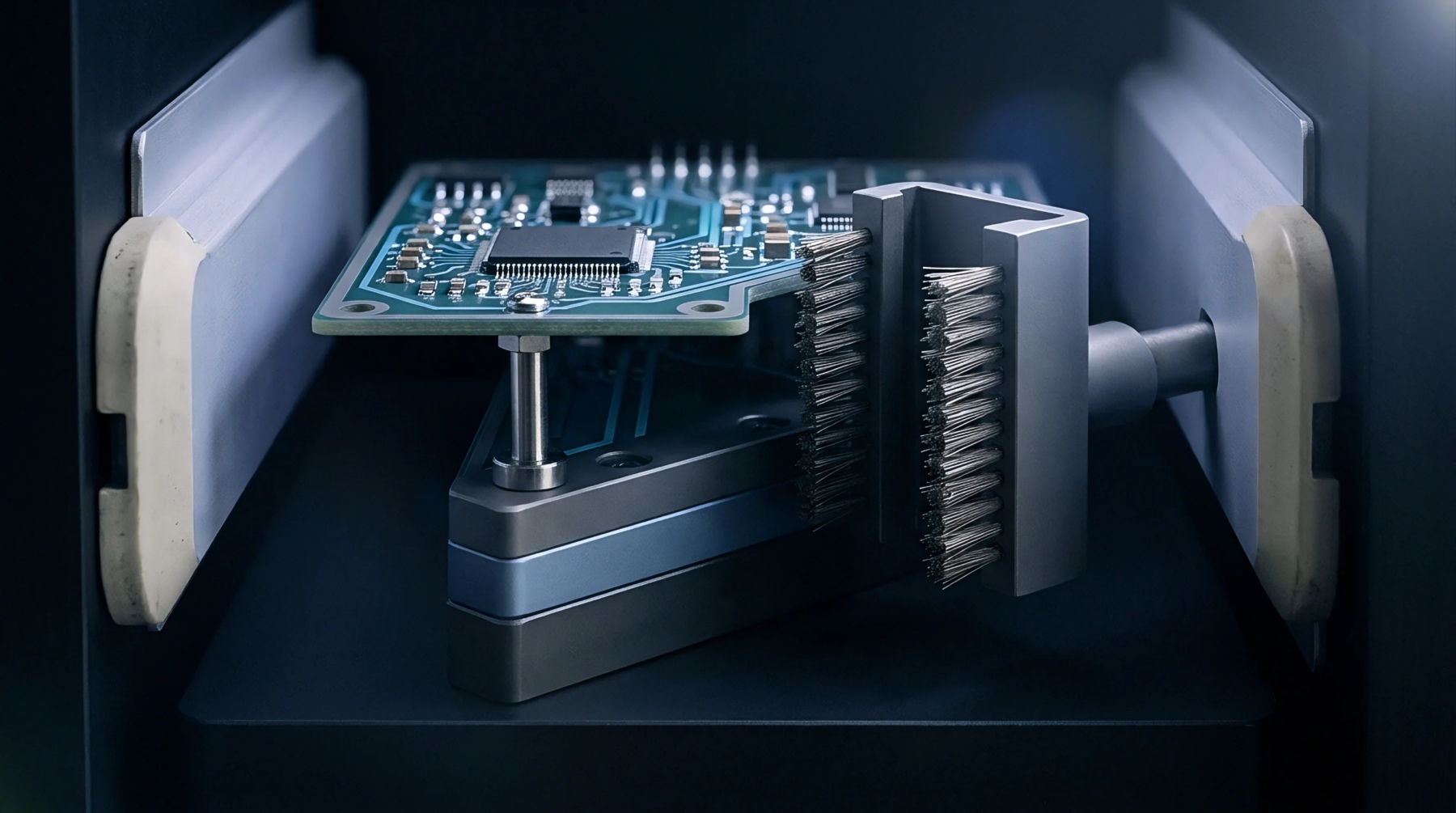
Unscreened high-frequency channel structural escapes drive PCI Express residual bit error rates above spec limits by inducing localized signal resonances.

Boundary scan access limits require balancing physical probe suppression against quantitative fault escape risks in high-density logic clusters.

Allocating latent defect risk in advanced assembly relies on defined screening limits, clear warranty triggers, and empirical root-cause testing formulas.
Intermetallic growth control and thermal profile validation prevent latent BGA fracture defects before boards leave the line.
Surveillance compliance demands continuous cross-tier test record alignment, analytical material validation, and strict engineering change authorization.

Unprobed high-speed nets demand combined boundary scan and thermal screening to bound latent defect escape liabilities before batch signoff.
Extrapolating high-temperature laminate loss tangent shifts prevents gigahertz plane edge emissions escapes caused by thermal cavity resonance shifts.

Sub-tier material drift erodes high-reliability board margins; mathematical risk modeling and rigorous chemical dossier validation eliminate latent field escapes.
Cyclic thermal loading degrades epoxy shear modulus, causing strain transfer loss that demands strict bondline guard-banding in technical files.
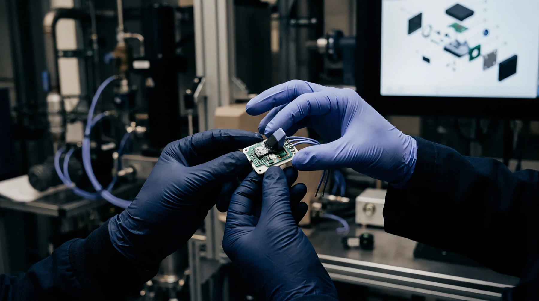
Dynamic four-wire testing isolates ambient and transient microvia resistance shifts during thermal stress to catch latent target pad defects before shipment.
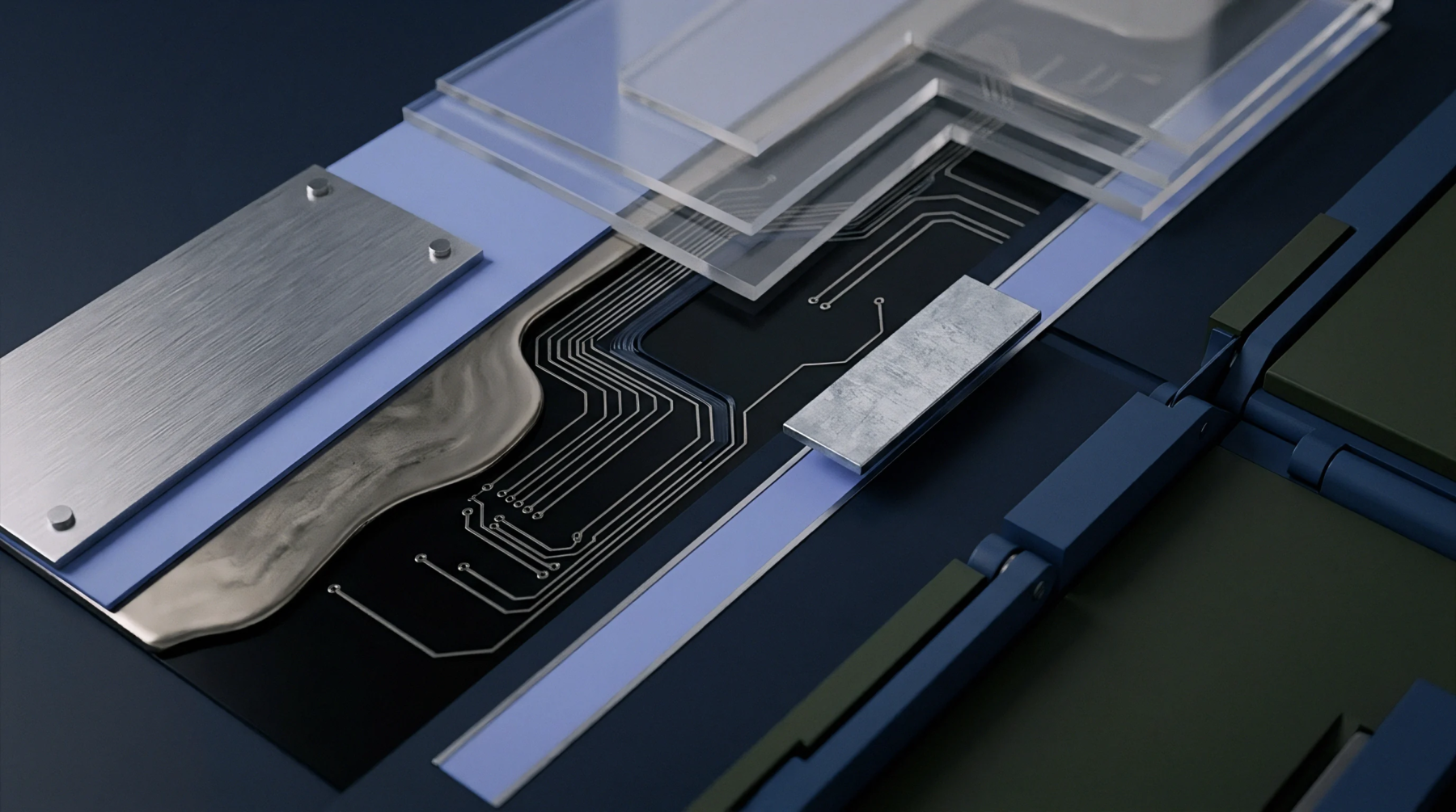
Microvia plating fatigue under thermal cycling stems from z-axis CTE mismatch, requiring ductile copper plating and continuous resistance monitoring to prevent field failures.
Weibull shape and location parameters derived from microsections quantify true target pad clearance safety margins, protecting buyers from latent dielectric field failures.

Asymmetrical dielectric buildup increases microvia thermal strain energy density, accelerating fatigue fracture at target pad corners during reflow cycling.

Asperity contact pressure above ten megapascals masks interface delamination during acoustic qualification, requiring thermal-bias ultrasonic verification.
Substrate fatigue crack propagation rates depend on mode mixity and resin compliance, requiring continuous in situ resistance logging to prevent field escapes.

Environmental temperature and humidity cycling degrades substrate integrated waveguide cavity damping by elevating loss tangents and fracturing via fences.

Differential channel skew drifts under environmental screening due to glass weave expansion mismatches, requiring in situ de-embedded phase verification.
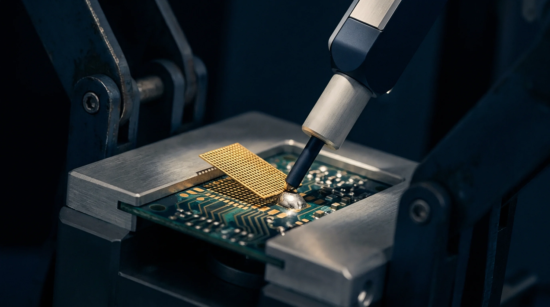
Verify structural fault coverage on high density assemblies by combining boundary scan with radiographic inspection where physical probe access falls below eighty percent.

Boundary scan preconditioning isolates constrained nodes without test pads, allowing analog signature analysis to verify passive and junction integrity.

Interfacial solder joint voids accelerate creep strain accumulation, converting IPC-compliant connections into latent field open circuits.
Controlled ENIG gold thickness between 0.04 and 0.07 micrometers prevents brittle intermetallic fractures and black pad failure on fine-pitch BGA assemblies.

Embedded IJTAG PRBS instruments run during stress screening capture transient interconnect failures that static functional bench tests miss.

Field return rates equal total screening escape rates scaled by operational duty cycle and environmental defect manifestation factors over time.

Converting Weibull distributions into warranty reserves requires multiplying quarterly wear-out failure fractions by landed costs and discounting net present value.

Waiving circuit test fixtures shifts latent defect risk to field warranty reserves unless compensated by boundary scan and verified thermal stress screening.
Loss tangent increases sharply near glass transition temperature, driving thermal eye closure and insertion loss drift that demand elevated-temperature coupon screens.

Weibull shape parameters below unity reveal latent microstructural interface escapes that pass zero-hour electrical testing but fail under thermal stress.

Modified counting sequence vectors compress boundary scan runs to logarithmic depth, isolating micro-bridges and cracked solder joints before field exposure.
Expertise is a utility, not a secret. sentiention™ publishes its working knowledge as open reference: intelligence layer covering the materials it sources, the markets it enters, and the reference that serves both.