Sub Terahertz Copper Roughness Modeling Using Atomic Force Power Spectral Density
Atomic force power spectral density models sub-terahertz copper loss by mapping nanoscale spatial frequency harmonics that standard profile metrics ignore.

Atomic force power spectral density models sub-terahertz copper loss by mapping nanoscale spatial frequency harmonics that standard profile metrics ignore.
Non-uniform cooling rates in multilayer presses induce anisotropic permittivity tensors, demanding multi-mode cavity extraction to prevent phase skew failures.
Integrating orthotropic dielectric tensors into full-wave solvers aligns simulated phase delay with production panels, eliminating scrap from unmodeled skew.

Calibrated two-port shunt-through VNA measurements require cable shield choke isolation and de-embedded fixture planes to resolve milliohm rail impedance accurately.

Rapid vacuum draw-down collapses convective heat transfer and destabilizes molten solder, demanding controlled depressurization rates below fifty millibars per second.

Anisotropic permittivity characterization isolates out of plane dielectric constants from in plane vectors to prevent high speed trace impedance mismatch.

Laminate dielectric thickness deviations alter power plane impedance and cavity resonance frequencies, driving radiated emissions past statutory EMC thresholds.
Perimeter via stitching suppresses plane edge radiated emissions by shunting RF displacement currents through low-inductance ground arrays before fields escape.

Plane cavity resonances create target impedance spikes that demand dampening vias, controlled ESR capacitors, and calibrated two-port VNA testing.
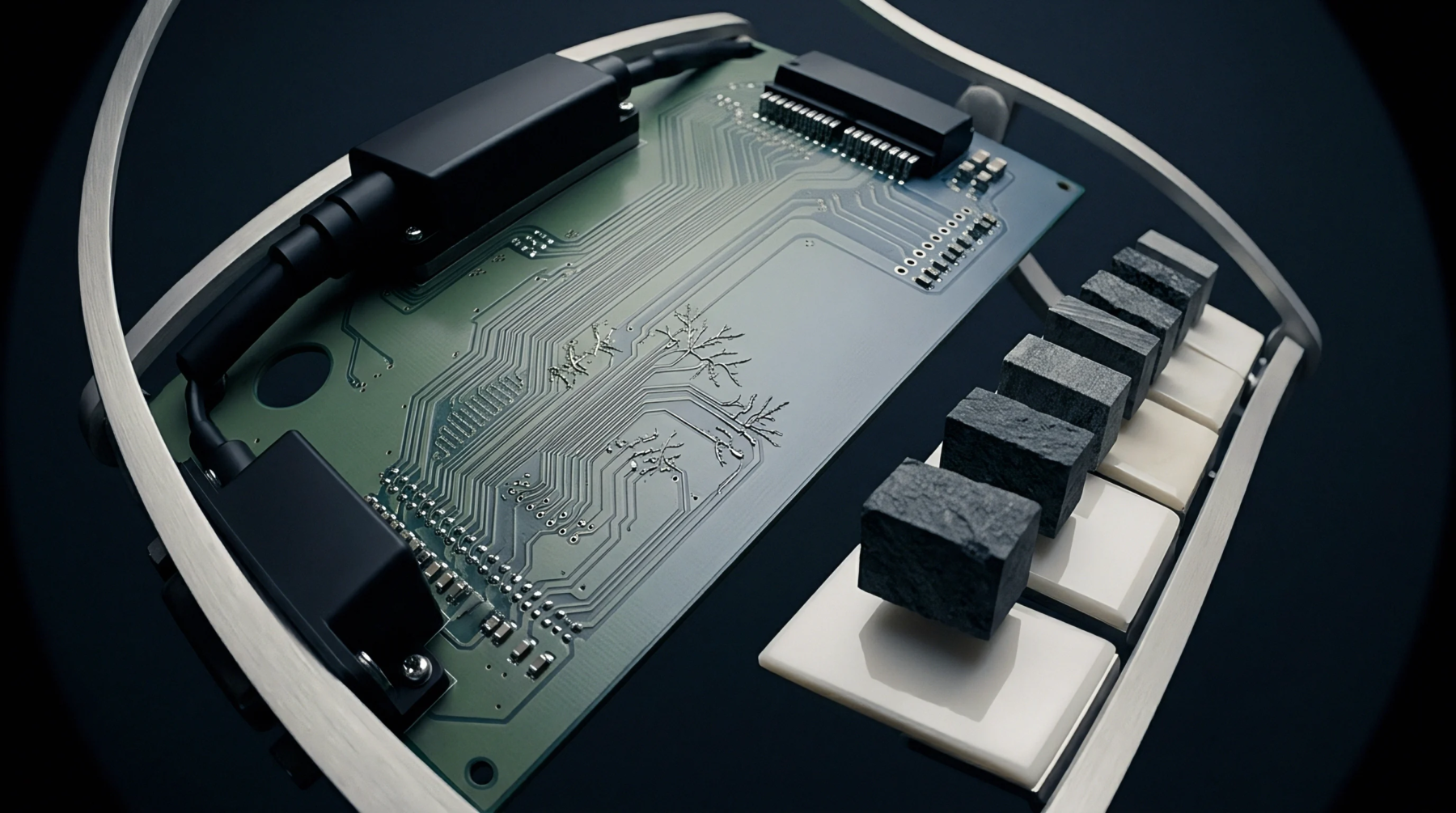
Etched sidewall taper concentrates high-frequency current into edge micro-roughness, doubling conductor losses above 50 GHz unless controlled by mSAP.
Maximize convection gas velocity and lower-plenum thermal bias to collapse cross-board temperature deltas on heavy copper stackups without slowing line output.
Calculate differential stripline impedance by substituting an etch-adjusted effective width and crown spacing into 2D field models before stackup release.
Etched PCB traces form trapezoids rather than rectangles; uncompensated sidewalls lower impedance by up to 4 ohms and amplify skin-effect losses above 10 GHz.

Dynamic optical spatial alignment compensates for non-linear carrier shrinkage during coreless production, preserving sub-micron overlay and multi-layer yields.
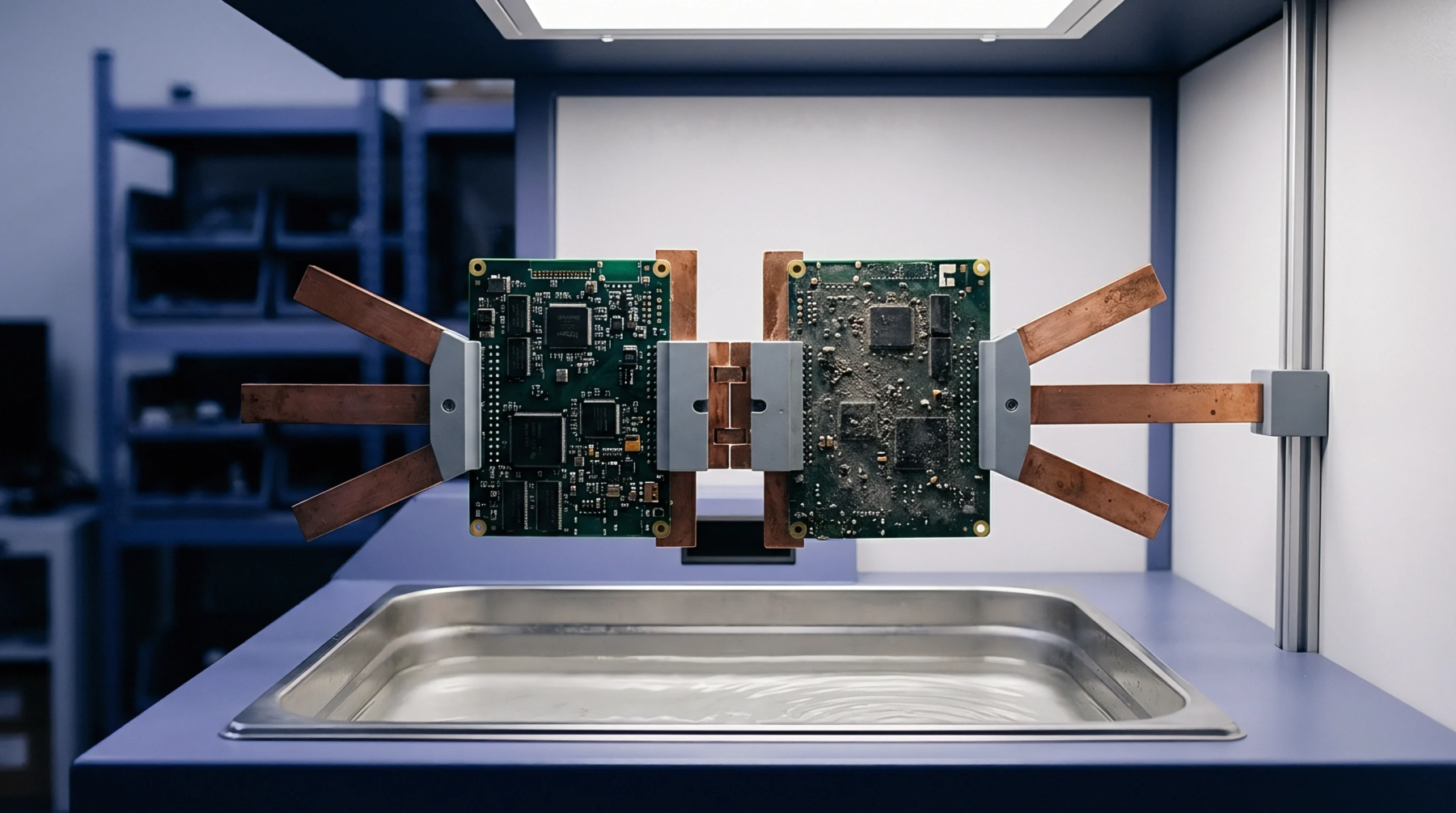
Non-linear spline algorithms mathematically eliminate localized PCB laminate shrinkage errors, securing sub-10 micron registration for reliable ultra-fine line microvia alignment.

Partial test sign-offs transfer strict product safety liabilities to importers, converting foreign factory testing gaps into uninsurable domestic regulatory exposure.
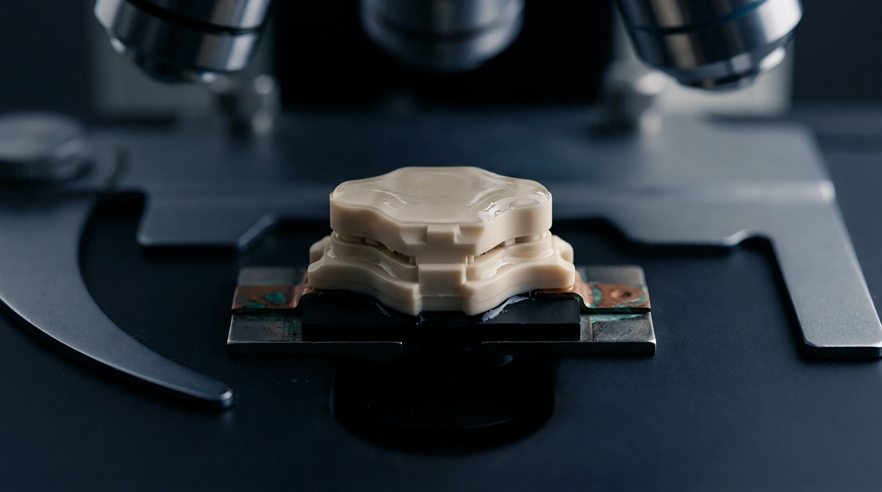
Waiving circuit test fixtures shifts latent defect risk to field warranty reserves unless compensated by boundary scan and verified thermal stress screening.
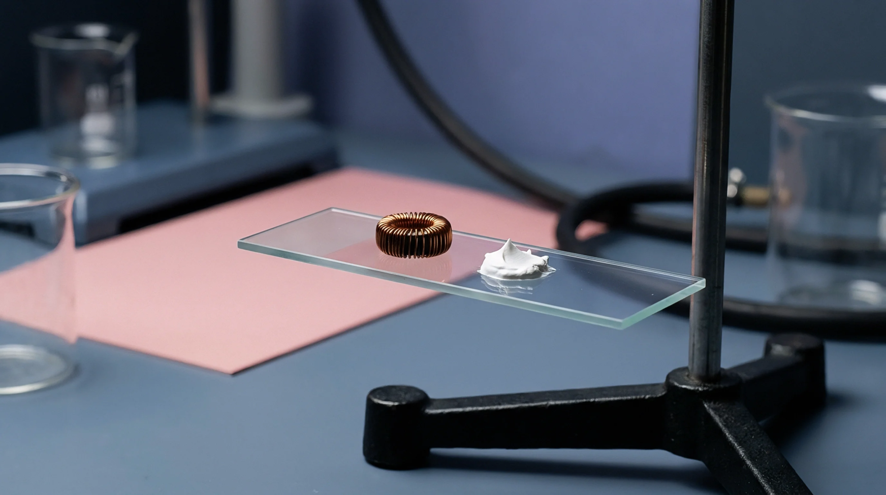
Contractual test waivers shift PCBA manufacturing liability to importers, requiring tight scope boundaries, price credits, and destination intake screening.
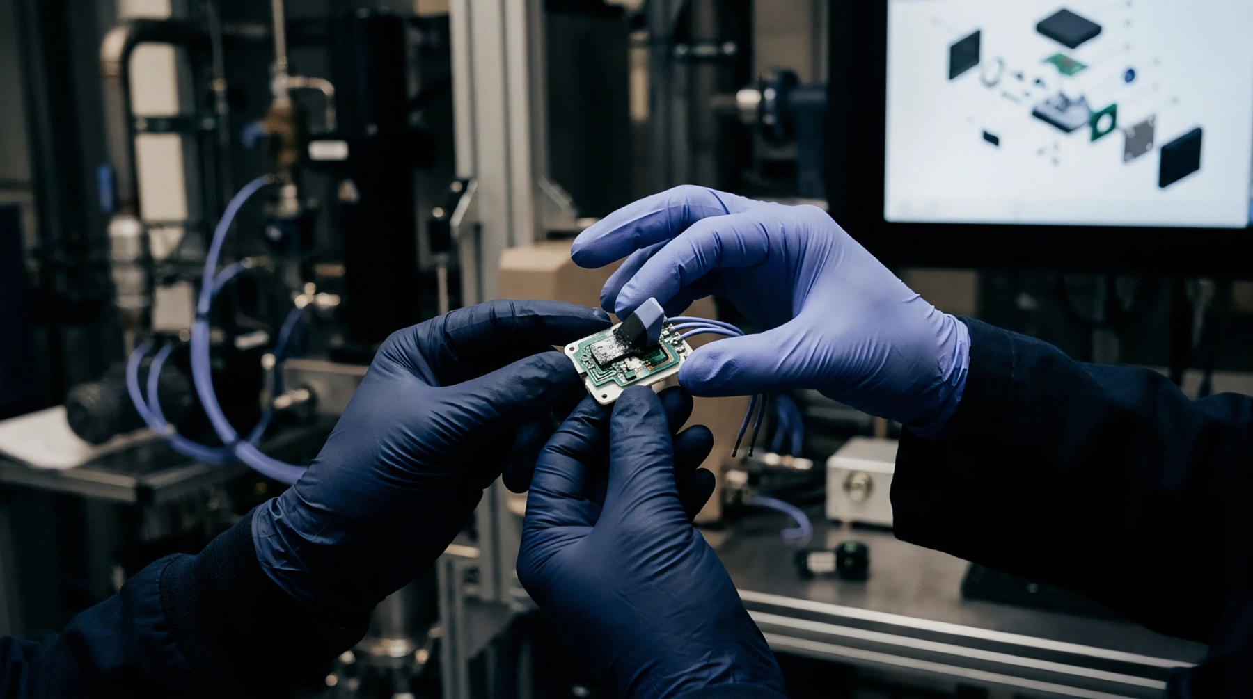
Predict long-term out-of-band field escape by modeling submicron plating fractures as dynamic slot radiators driven by thermal fatigue and harmonic currents.
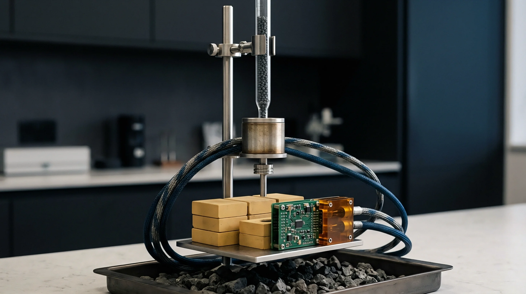
Dedicated in-circuit test fixtures achieve break-even only after board layouts survive frozen production volumes that fully absorb initial tooling charges.
Fixtured in-circuit test amortizes its nonrecurring tooling against flying probe runtime rates when production batches exceed twelve hundred double-sided boards.
In-circuit testing crossover volume thresholds occur where amortized fixture tooling costs intersect flying probe machine hour charges, typically near 5,500 units.
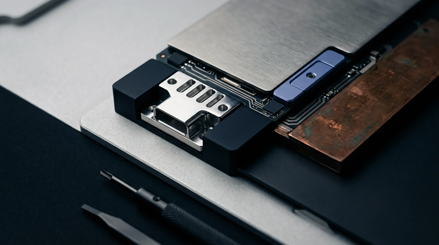
Managing reflow on high thermal mass PCBs requires extended soak profiles, nitrogen inerting, and precise TC placement to hold Delta T below ten degrees Celsius.
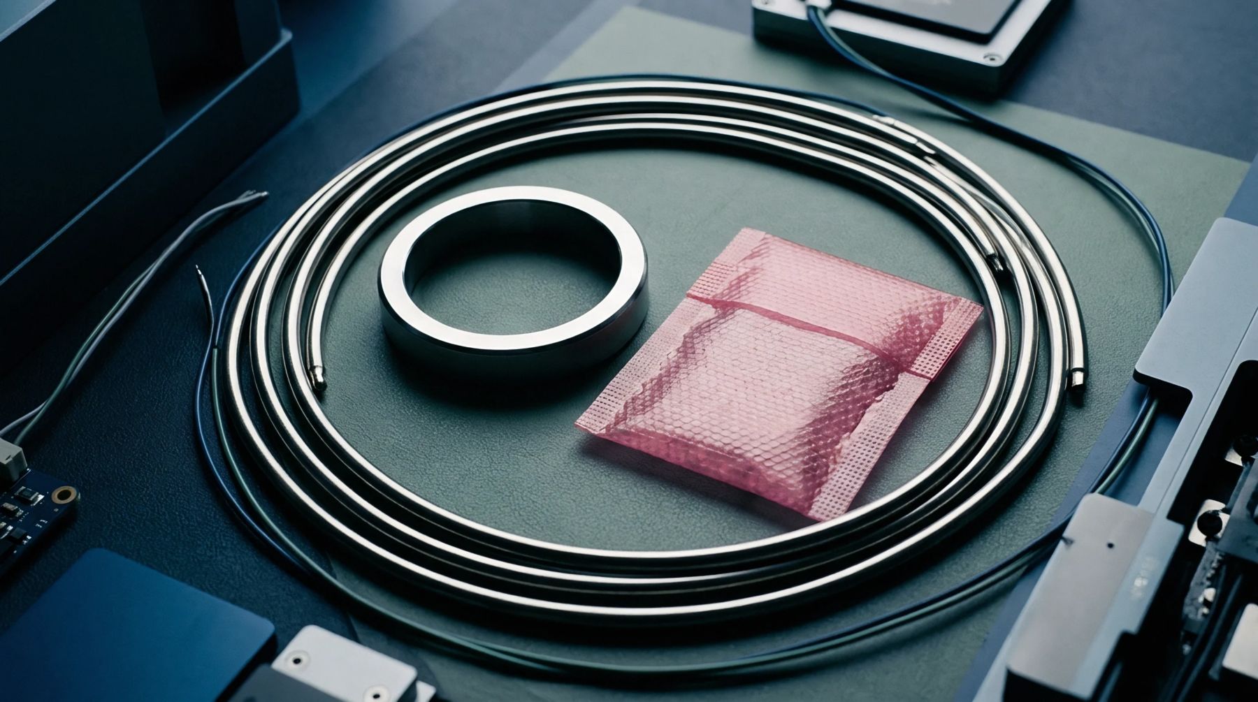
Micro-turbulent nitrogen convection increases heat transfer coefficients to 85 W/m²·K, requiring tight velocity control to avoid component displacement.

Substrate panel deformation stems from thermomechanical mismatch, cure shrinkage, and copper asymmetry, requiring balanced layouts and strict thermal control.
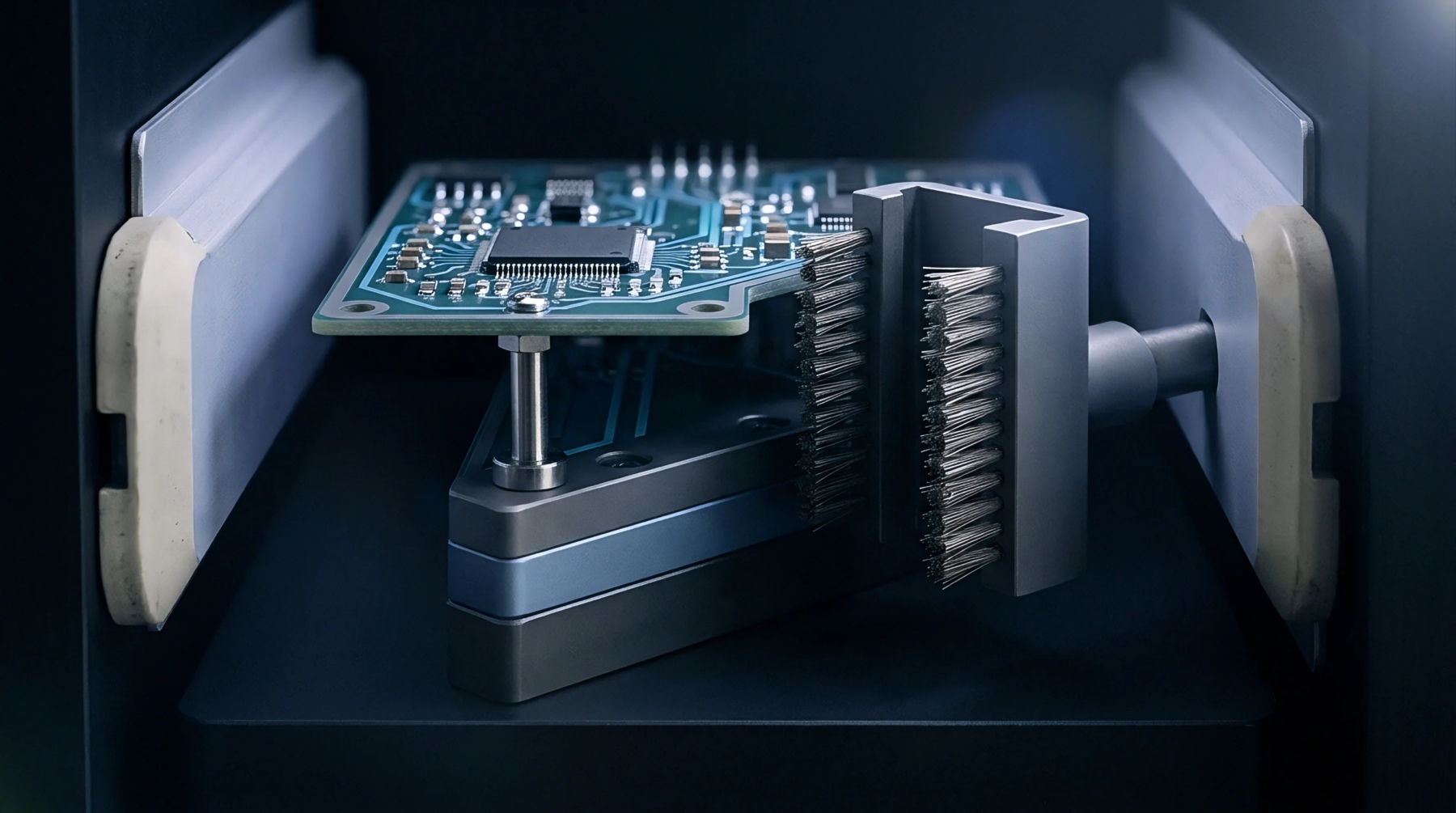
Thick boundary layers behind tall, high-mass SMT packages insulate joints from oven gas, creating steep thermal deltas that force slower line speeds.
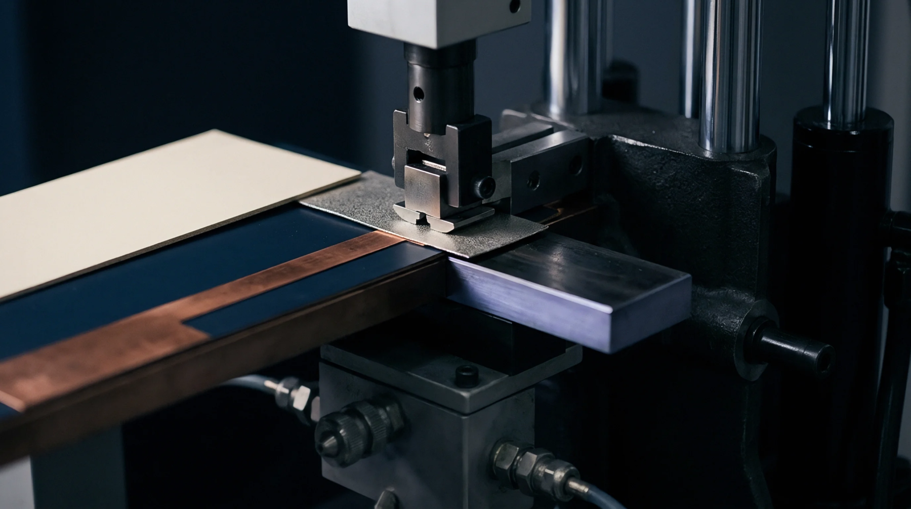
Non-linear interphase polarization causes unmodeled phase drift in sequential multilayers; accounting for this gradient restores millimeter-wave array yields.

Forced convection reflow zones transfer thermal energy by breaking stagnant boundary layers with gas jets calibrated between two and six meters per second.

Sequential press cycles alter resin fill and weave orientation, shifting out-of-plane permittivity by up to nine percent and throwing microstrip impedance off target.
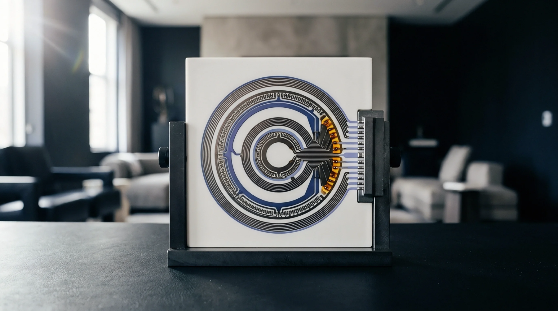
Dielectric relaxation drives high-frequency core attenuation through phase-lagging dipoles, requiring causal modeling and hybrid stackups to balance board costs.
Expertise is a utility, not a secret. sentiention™ publishes its working knowledge as open reference: intelligence layer covering the materials it sources, the markets it enters, and the reference that serves both.