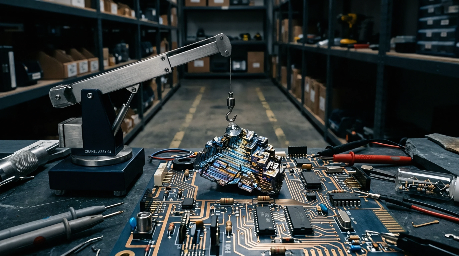
Glass Style Selection for Controlled Impedance Printed Circuit Boards
Specify mechanically spread, dual-ply glass styles to eliminate weave windows, suppress phase skew, and maintain consistent characteristic impedance.
Specify mechanically spread, dual-ply glass styles to eliminate weave windows, suppress phase skew, and maintain consistent characteristic impedance.

Correct coupon placement in panel margins guarantees accurate impedance testing and microsection validation while maximizing usable board yield.

High density SMT pad parasitics cause local impedance drops up to 12.8 Ohms, requiring TDR coupon extraction and de-embedded S-parameters to verify signal limits.
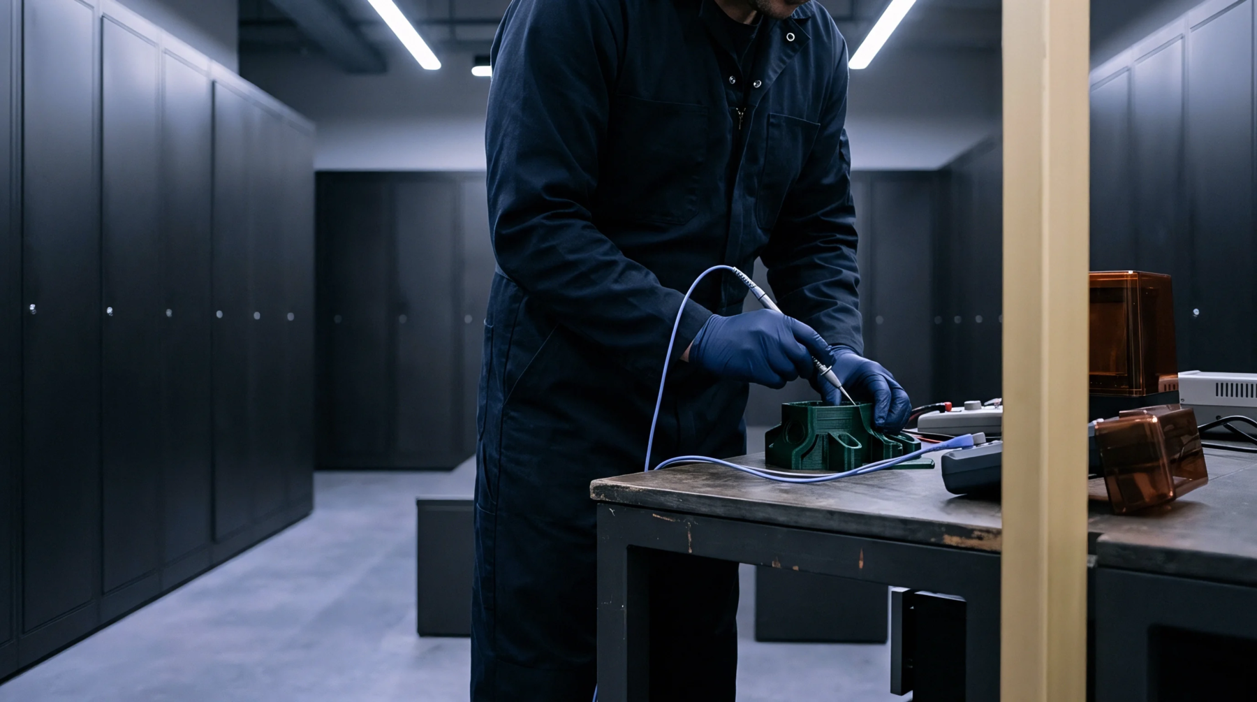
High-speed functional testing validates SerDes signal integrity via calibrated de-embedding, dynamic eye-margin capture, and tight thermal regulation.
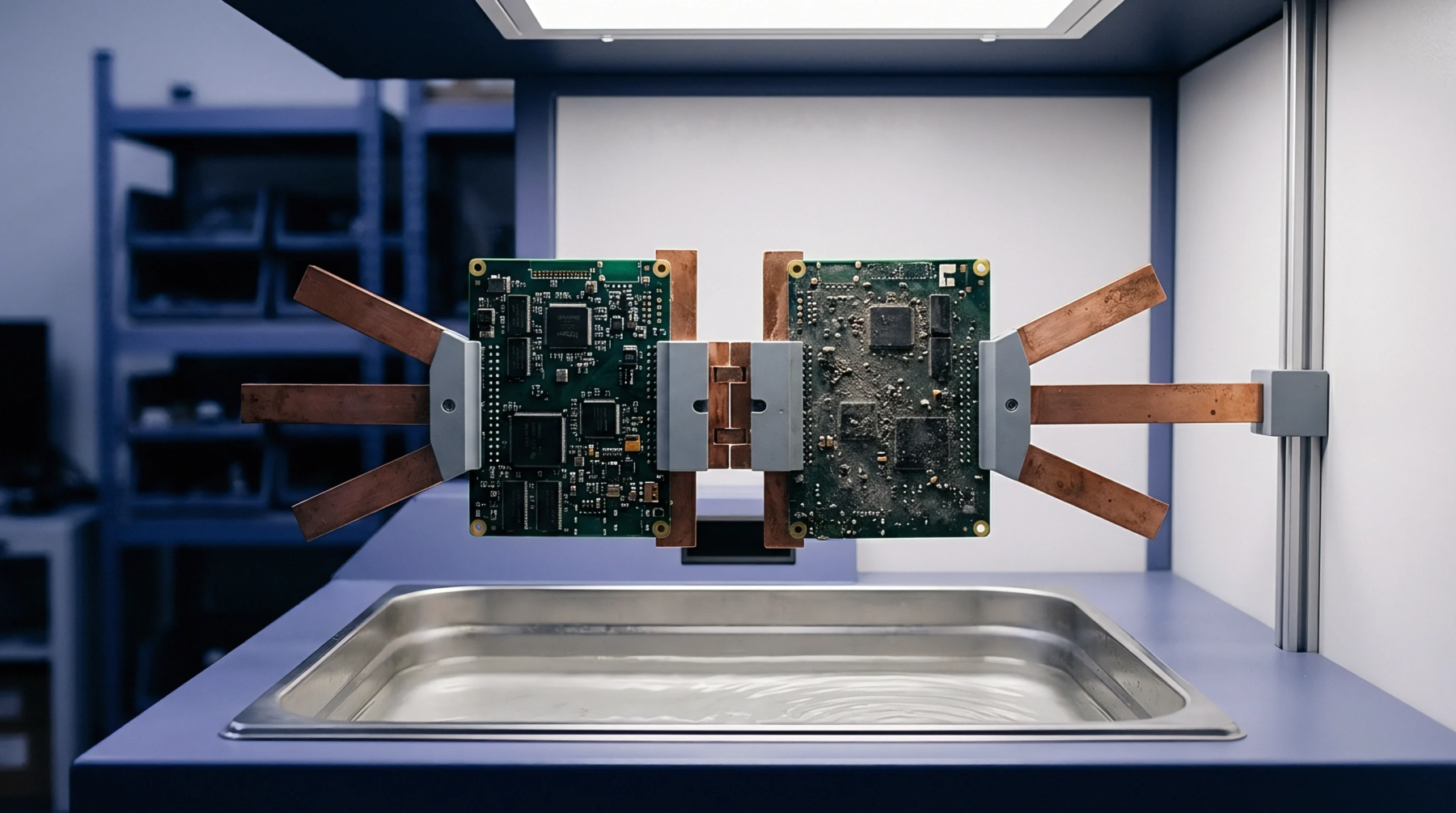
Verify serial capacitor array solder joints using 3D X-ray, high-frequency TDR, and in-situ thermal electrical monitoring to catch sub-micron cracks before field failure.
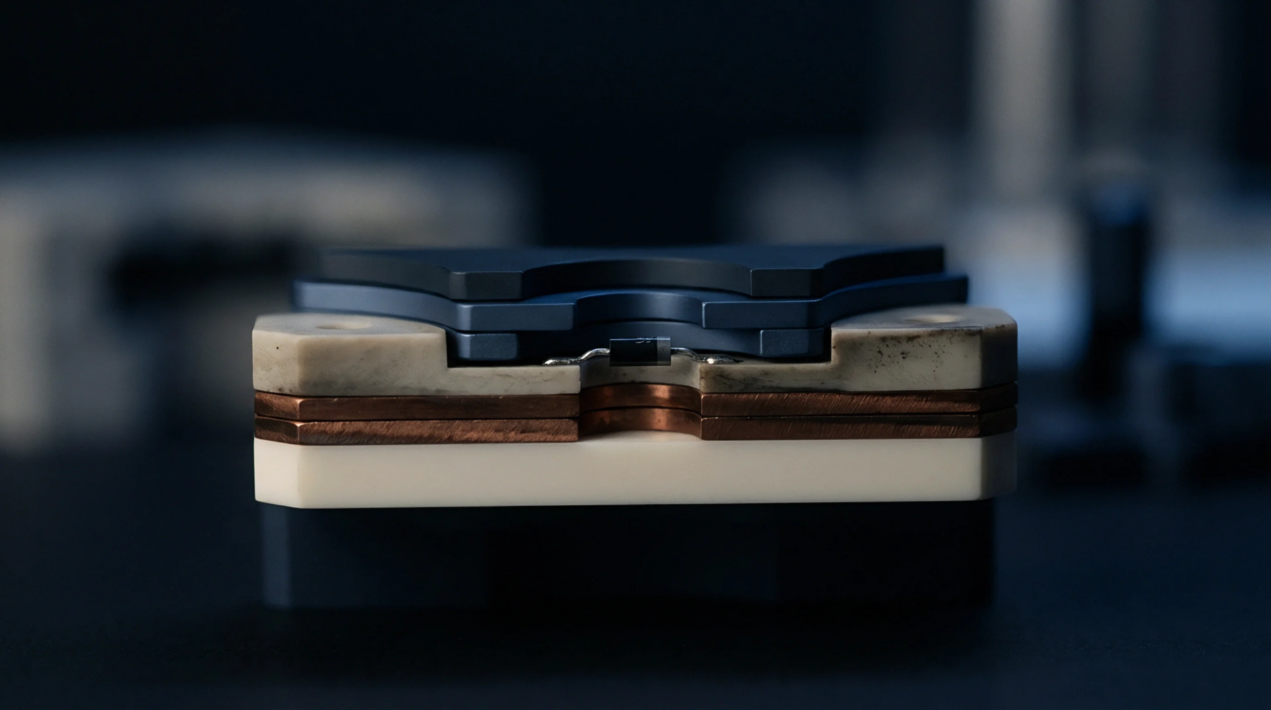
Near-field coupling across micro-split planes increases return loop inductance and converts differential signals into common-mode emissions.
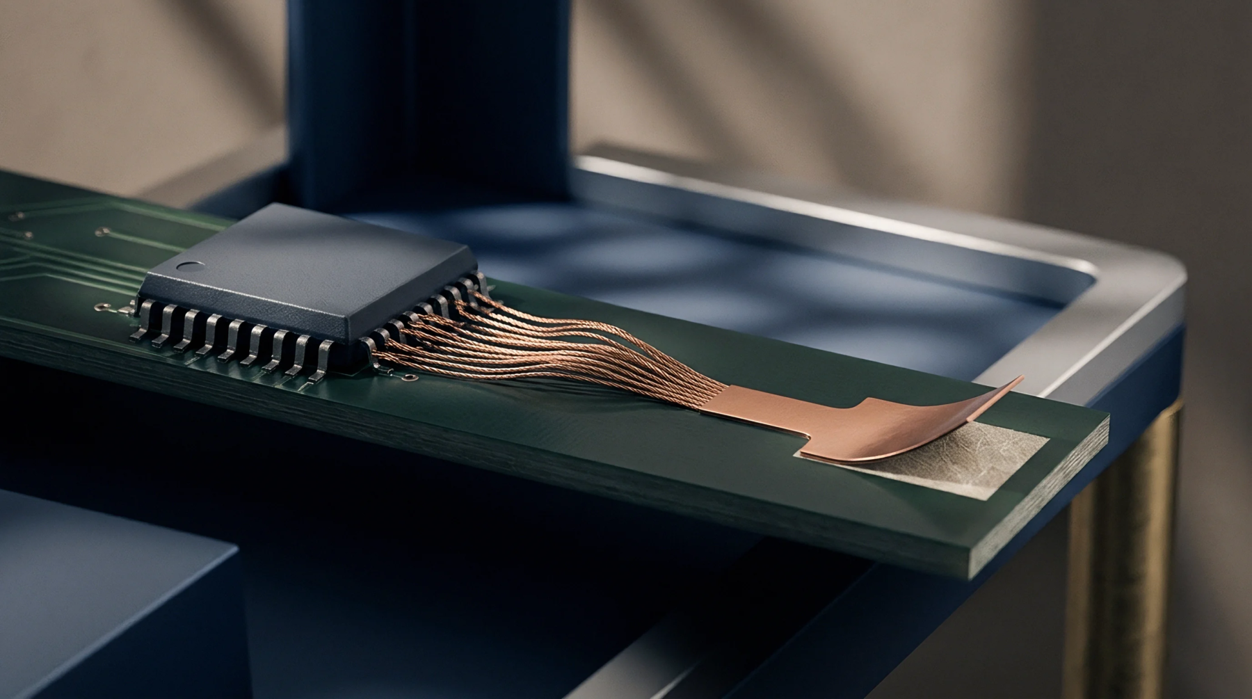
Unstitched ground plane slots in HDI boards cause severe impedance spikes, eye collapse, and radiated emission test failures across high-speed serial channels.
Target impedance modeling defines maximum power rail impedance limits across frequency to suppress transient voltage ripple through thin plane cavity stackups.
Anisotropically compensated dielectric modeling prevents impedance errors and differential skew drift across multi-press sequential HDI stackups.
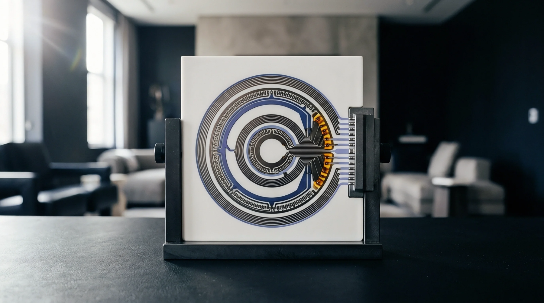
Optimizing test lands requires balancing parasitic capacitance below 0.15 pF with board strain limits under 500 micro-strain during in-circuit probing.
Calibrating HDI propagation delay demands de-embedding test fixture launches and extracting frequency-dependent permittivity from real coupon return geometries.
Quantifying sub-tier PCB laminate variations mandates panel-level TDR coupon screening, IPC-6012E microsection verification, and explicit master roll lot traceability.
Test point parasitic capacitance creates localized low-impedance discontinuities that increase insertion loss and jitter on high-speed PCB traces.
Phase-separated ground layers limit transient extraction through local dielectric polarization saturation and microvia current crowding under high di/dt loads.
Electromagnetic coupling and impedance discontinuities in aging probe arrays stem from tip wear, force decay, and inter-pin crosstalk that degrade high frequency test accuracy
Differential phase skew standards require de-embedded S-parameter phase extraction or calibrated TDR thresholding over spread-glass coupons to verify limits.
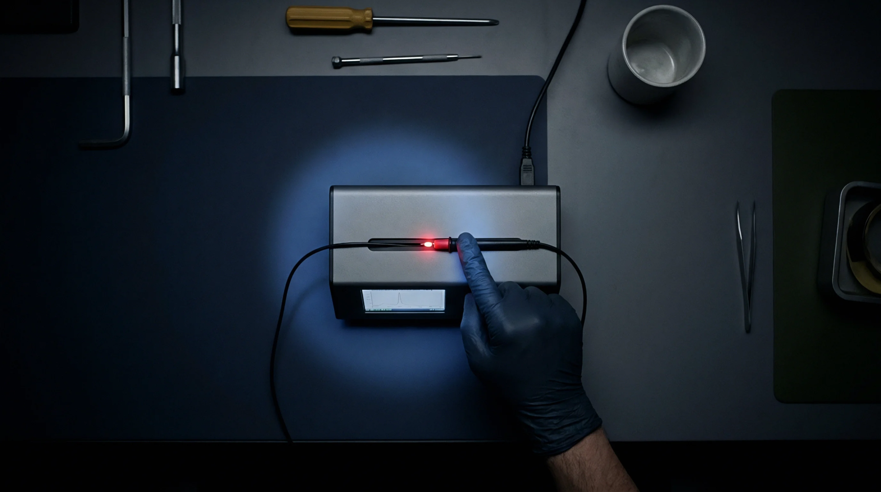
Guardbanding high-density interconnect audits requires four-wire Kelvin sensing and high-frequency reflectometry to catch latent microvia opens before reflow.
Microsectioning and cavity resonator perturbation isolate glass bundle pitch drift and resin window skew before committing high-frequency panels to volume drill.
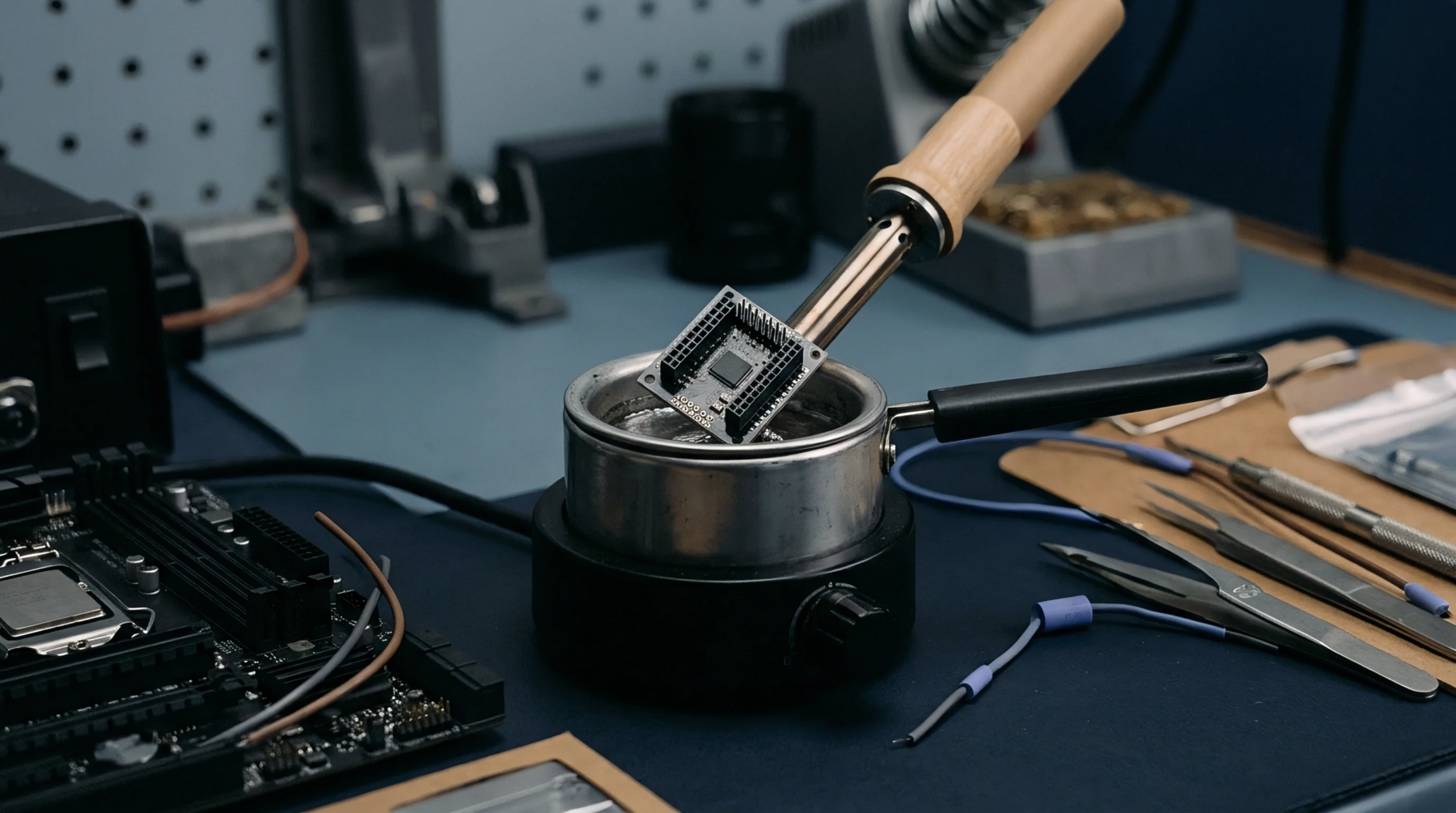
Diagnostic labor caps balance technician hourly payroll against scrap value to prevent unprofitable rework cycles on defective printed circuit board assemblies.
Perimeter via stitching suppresses plane edge radiated emissions by shunting RF displacement currents through low-inductance ground arrays before fields escape.
Calculate differential stripline impedance by substituting an etch-adjusted effective width and crown spacing into 2D field models before stackup release.
Dynamic flexure drives interfacial tooth fracture and polymer relaxation, raising millimeter-wave attenuation long before DC resistance detects trace fatigue.
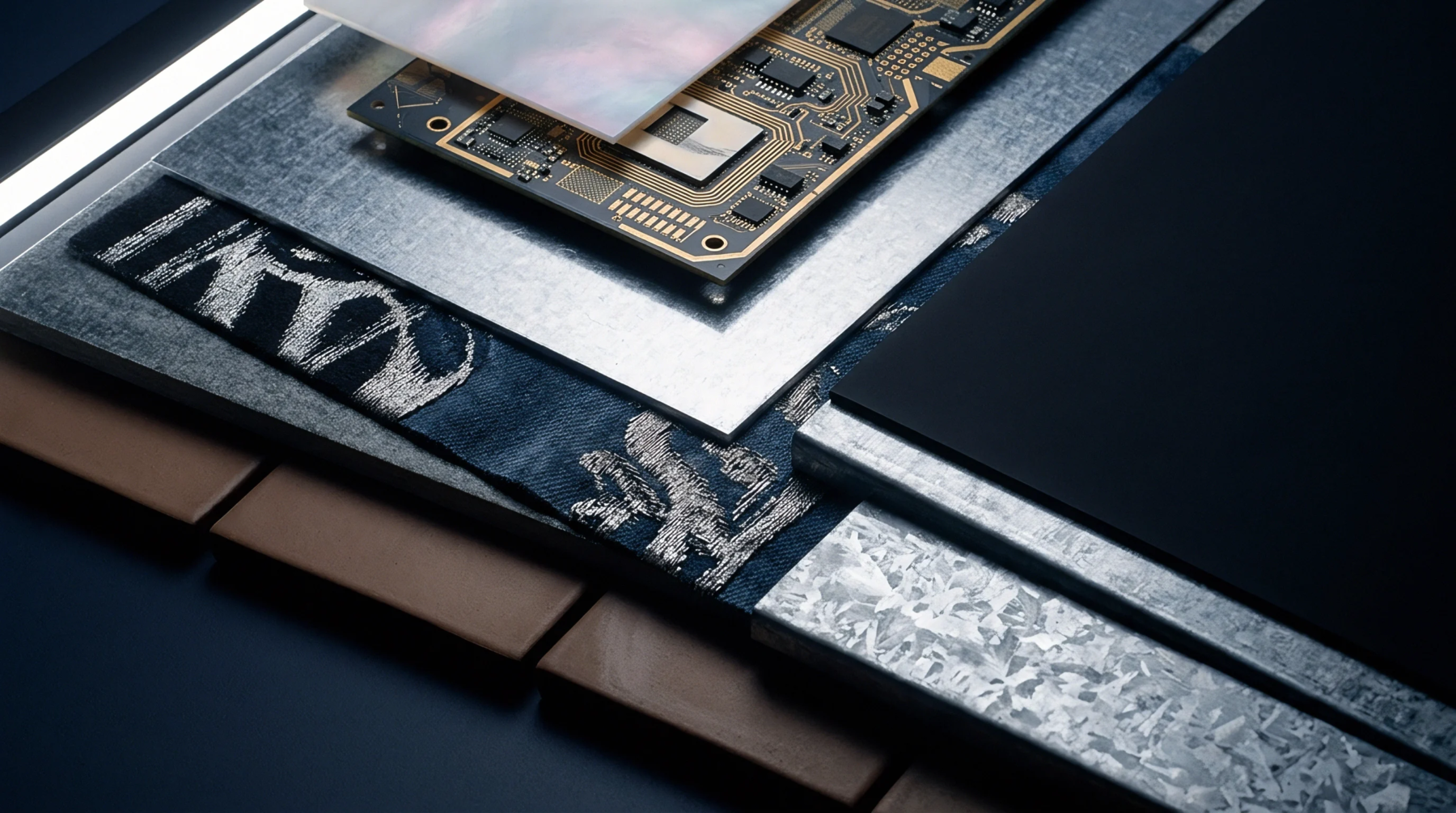
Mitigating microstrip phase delay variation demands combining spread L-glass prepreg with off-axis trace routing and strict fab drawing reinforcement notes.
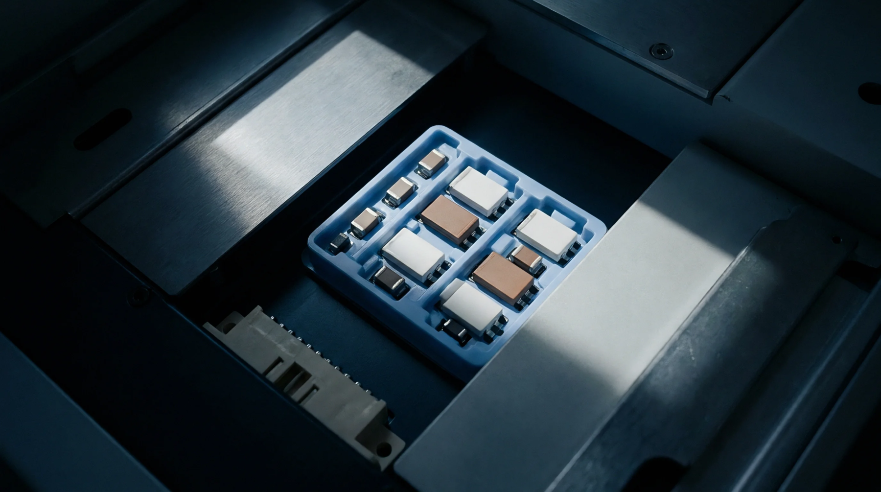
Reference plane splits add localized loop inductance that depresses resonant emission frequencies, turning functional clock harmonics into compliance failures.
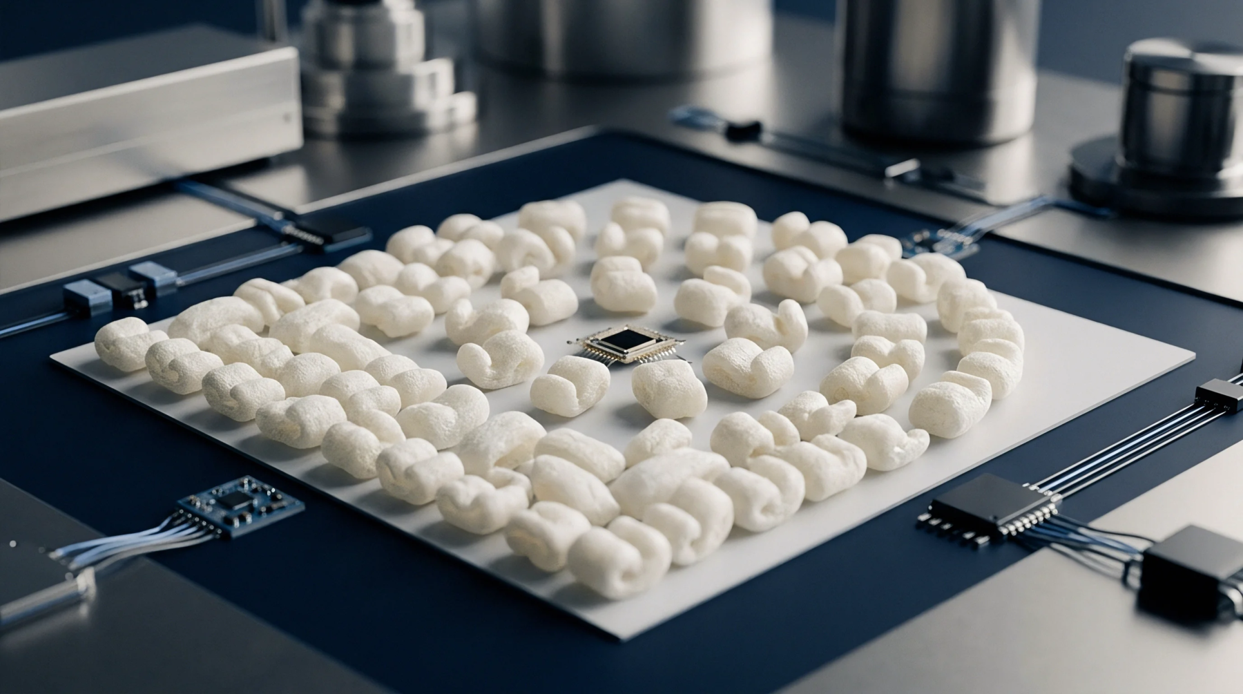
Planar microvoids exceeding eight percent along solder perimeter boundaries trigger severe impedance mismatches, inducing high-frequency PAM4 eye diagram closure.
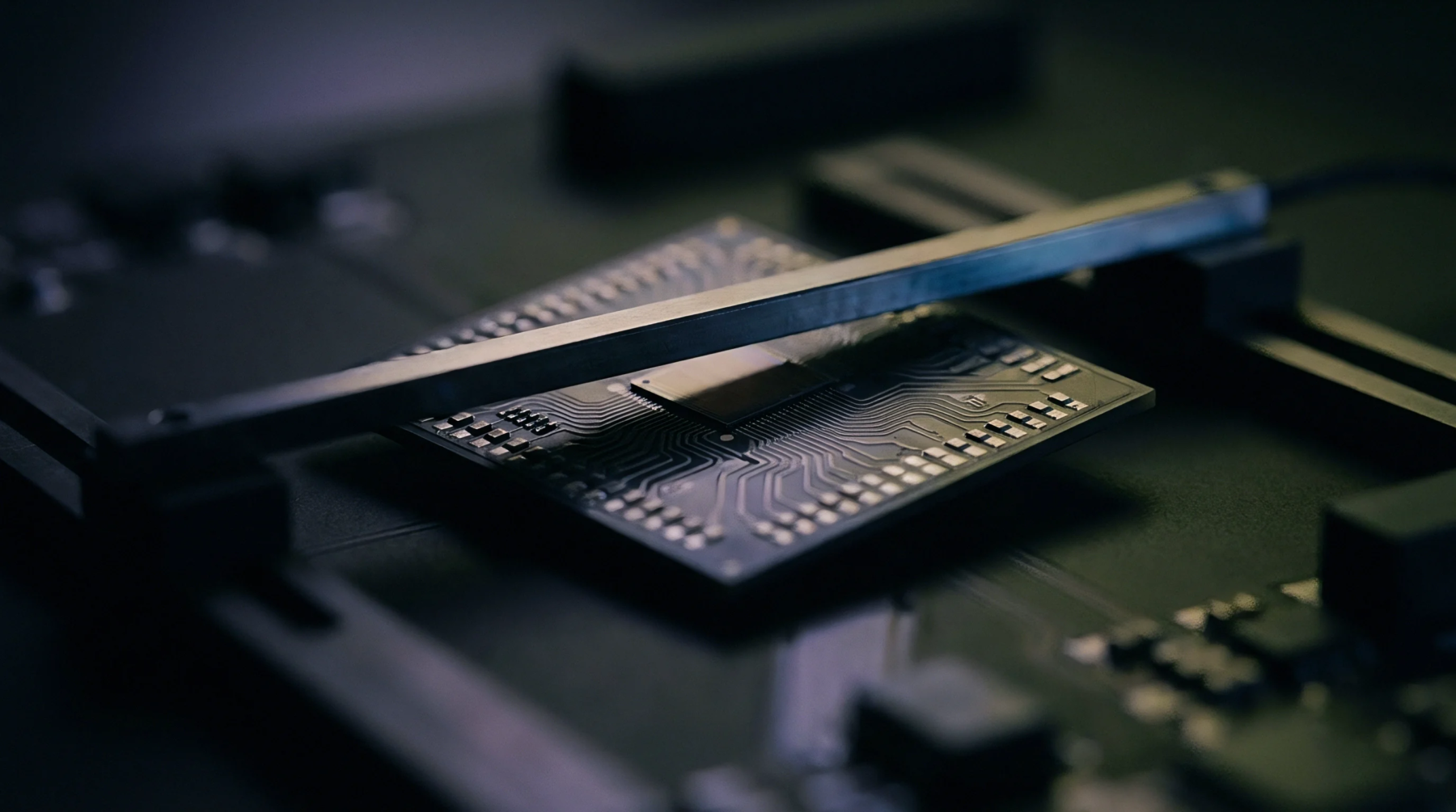
Gigahertz line discontinuities escape static boundary scans; isolating impedance dips, stubs, and microcracks demands sub-twenty picosecond reflectometry.
Latent substrate microcracks close elastically at room temperature, escaping DC continuity tests until thermal expansion separates the fractured interfaces.
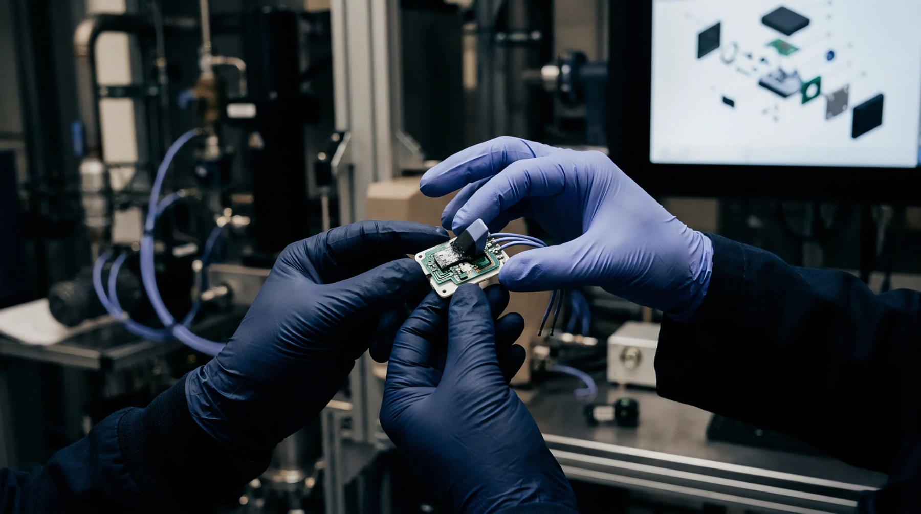
Electroless copper seed thickness variations widen flash etching dwell times, causing severe lateral undercut, collapsed etch factors, and impedance scrap.
Modeling AC-coupled scan channels requires combining IEEE 1149.6 low-frequency pulse decay with microwave pad parasitics to stop latent defect escapes.
Fine line HDI etching yield hinges on managing lateral undercut through thin copper foils, uniform fluid spray dynamics, and semi-additive process transitions.
Expertise is a utility, not a secret. sentiention™ publishes its working knowledge as open reference: intelligence layer covering the materials it sources, the markets it enters, and the reference that serves both.