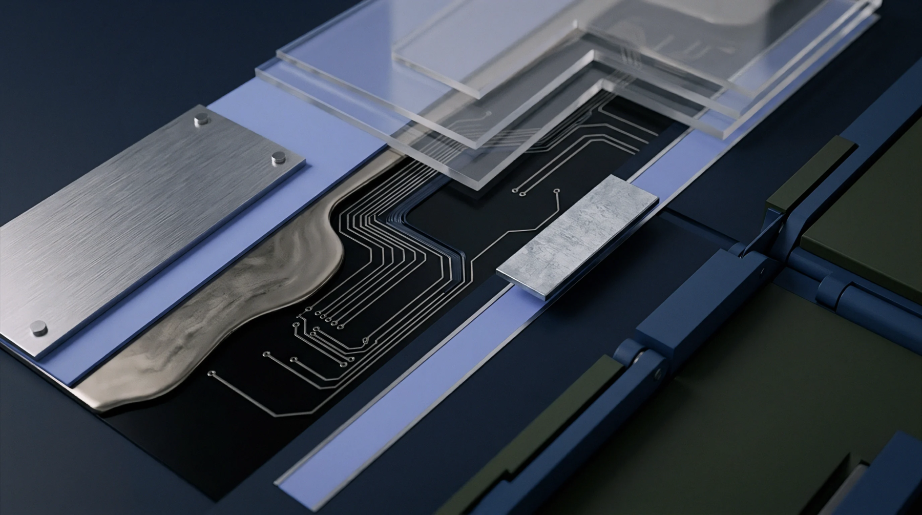
Impedance Coupon Reports Read against the Working Board
Peripheral coupon TDR reports require empirical offset adjustments derived from physical microsections to accurately reflect functional internal board impedance.
Peripheral coupon TDR reports require empirical offset adjustments derived from physical microsections to accurately reflect functional internal board impedance.

Adhesiveless hydrophobic polyimide interfaces reduce high-frequency dielectric attenuation by suppressing moisture uptake and eliminating lossy acrylic adhesive layers.
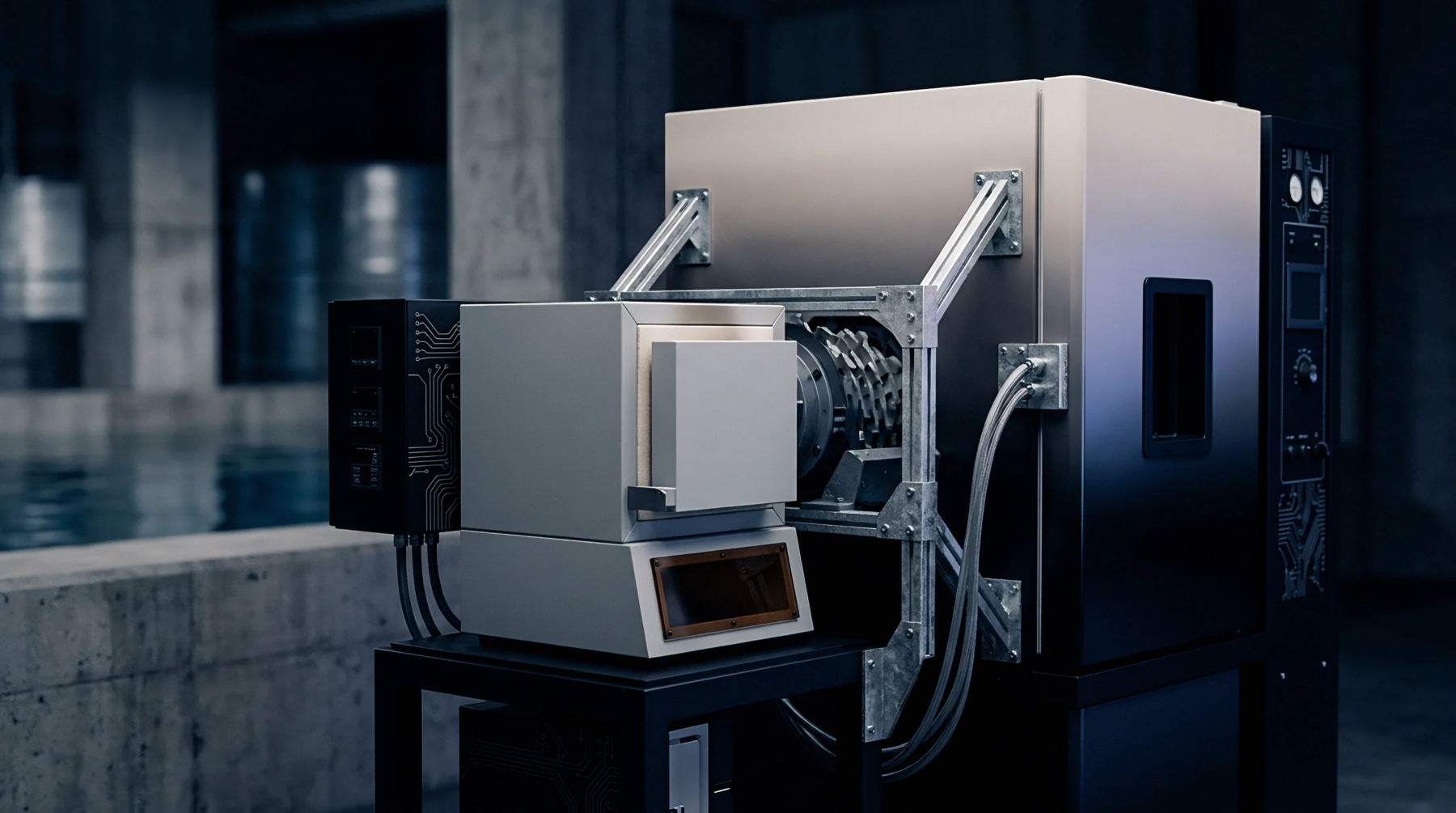
Argon cluster beam sputter rates drop up to 30 percent across crystalline Ni3P boundaries in amorphous Ni-P, requiring dynamic phase calibration to prevent barrier layer thickness overestimation.
Substrate copper roughness exceeding skin depth dampens cavity quality factor by extending surface current paths, demanding 3D surface area profiling and incoming batch screening.
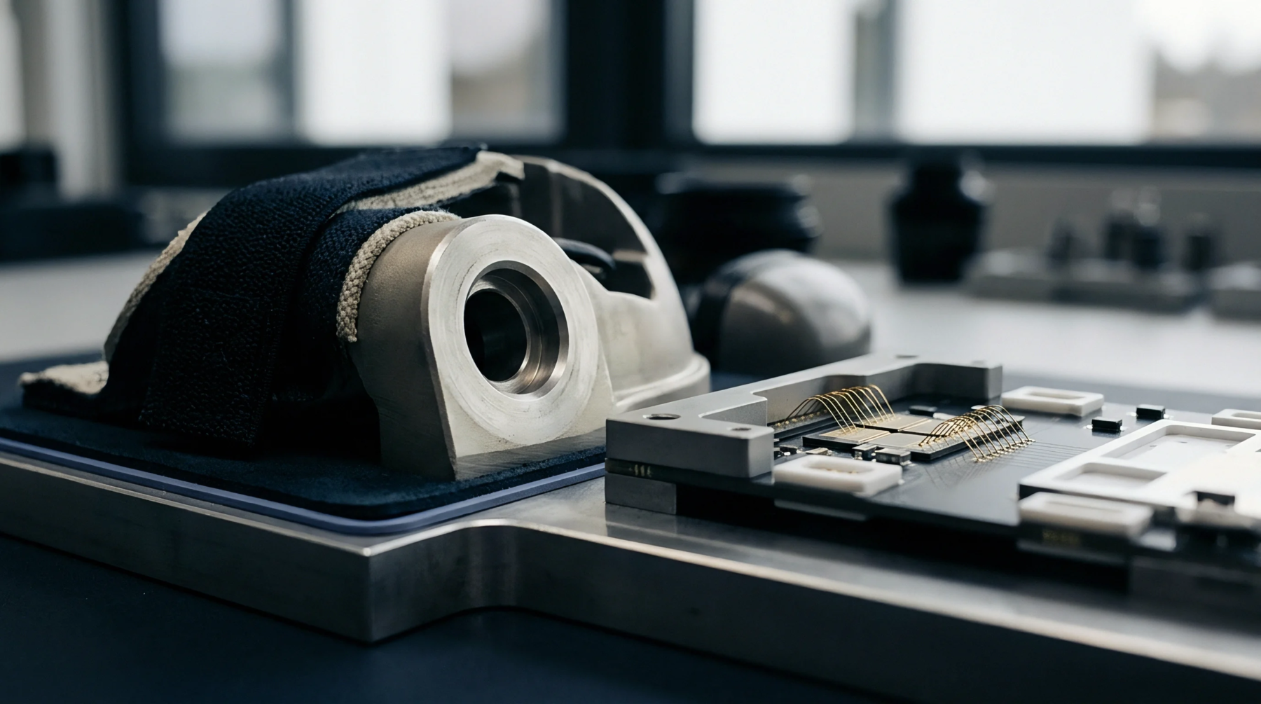
Calibrating optical inspection on sub-30 µm traces requires 3D slope profiling artifacts to prevent false line-width scrap driven by sidewall taper shift.
Air gap corrections eliminate systematic two to six percent dielectric underestimation in clamped stripline tests, preventing finished board impedance failures.
IPC-4101 slash sheets establish mandatory baseline physical, thermal, and electrical limits that override generic trade names to enforce material reliability.
mSAP yield optimization requires balancing electroless seed thickness tolerances within ten percent to prevent flash etch trace undercut and impedance failures.

Electroformed nickel stencils lower aperture wall roughness below 0.08 µm Ra, enabling clean solder paste release at area ratios down to 0.50 for 0.3mm BGAs.
Controlled impedance tolerance analysis maps resin content, foil roughness, and etch factors through RSS models to set yield-optimized fab drawing notes.
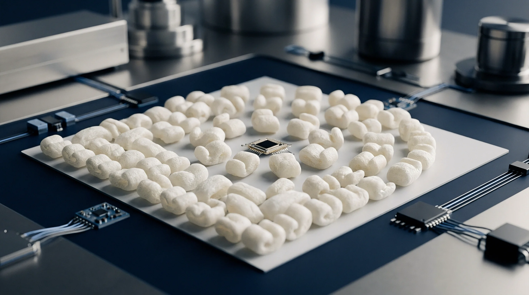
Parallel plate capacitance testing extracts packaging core permittivity from 100 Hz to 1 GHz by applying guarded electrodes to etched, preconditioned coupons.

Dielectric characterization methods determine in-circuit signal velocity by accounting for test fixture field structure, glass anisotropy, and copper surface roughness.
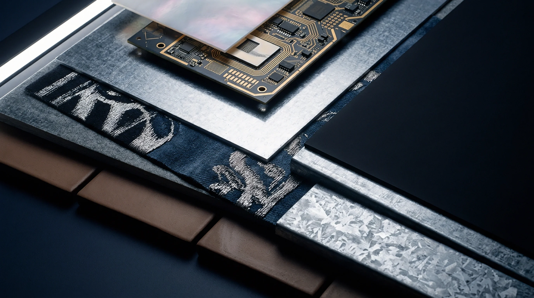
Quasi-optical extraction isolates intrinsic substrate loss from copper roughness, requiring explicit z-axis anisotropy conversion for accurate mmWave stackup design.

Structural strain transfer requires minimal bondline thickness, high shear modulus adhesives, and precise surface roughness matching to prevent measurement lag.
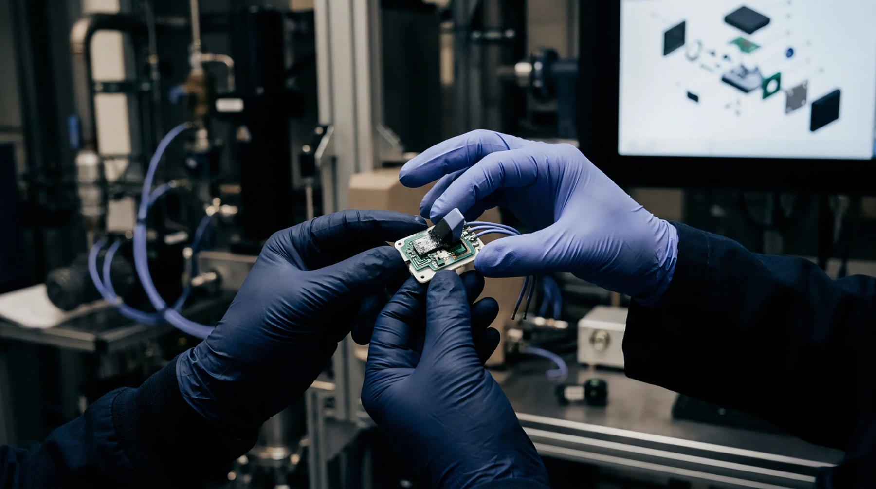
Non-linear viscoelastic cure modeling predicts microvia target pad separation by coupling resin shrinkage to interfacial cohesive fracture energy.

Step height verification on cluster-processed amorphous substrates requires guardbanded metrology and tip-force or dispersion compensation to prevent yield loss.
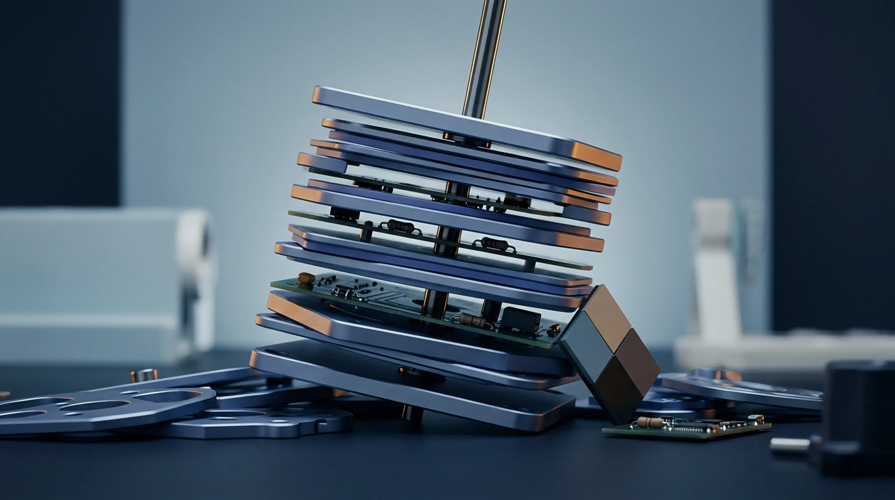
Copper surface roughness increases high frequency cavity conductor attenuation by extending skin current path length and degrading unloaded quality factor.
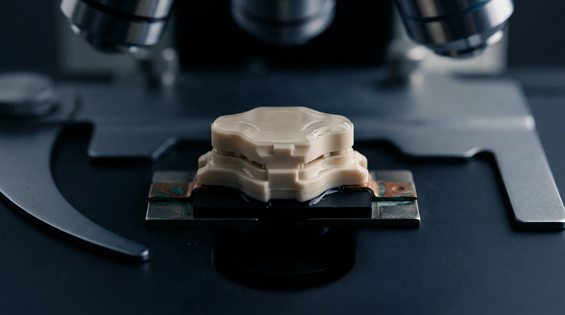
Spatial dielectric variation across organic package cores causes differential phase skew and impedance ripple, requiring spread glass and strict panel-level metrology.
Mid-loss laminates balance dissipation factors between 0.005 and 0.010 with moderate panel costs, matching PCIe Gen 4 and 10GbE signal integrity demands.
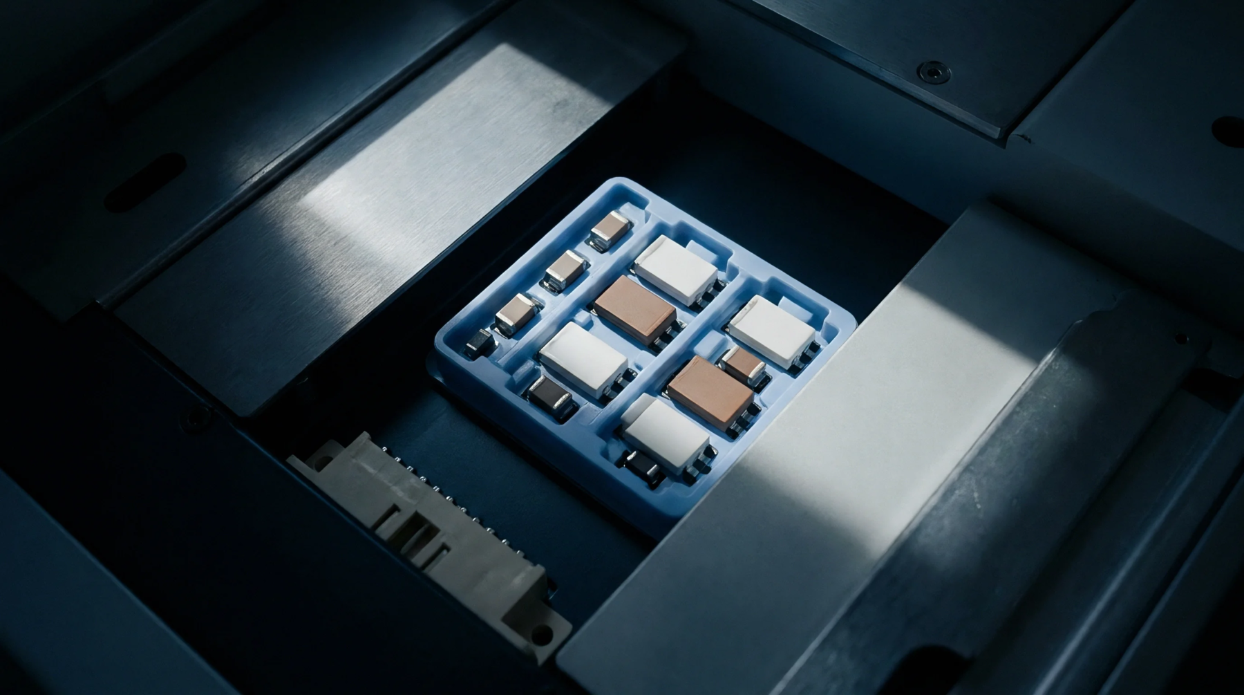
Etch fluid pooling creates trace asymmetry, changing high-frequency conductor profiles and driving insertion loss variations across printed circuit panels.
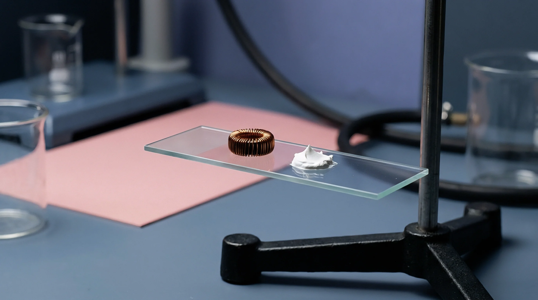
Differentiate foil roughness phase delay from glass weave skew by combining multiline TRL de-embedding with broadband phase-slope extractions on spread-glass coupons.
Sub-30 micron traces require 0.15 to 0.35 micron seed layers on ultra-smooth dielectrics, balancing high peel strength against rapid differential flash etching.
Environmental temperature and humidity cycling degrades substrate integrated waveguide cavity damping by elevating loss tangents and fracturing via fences.
Lead-free reflow elevates stripline phase delay by increasing polymer cross-linking and substrate permittivity, requiring tight furnace profiling and low-loss resin selection.
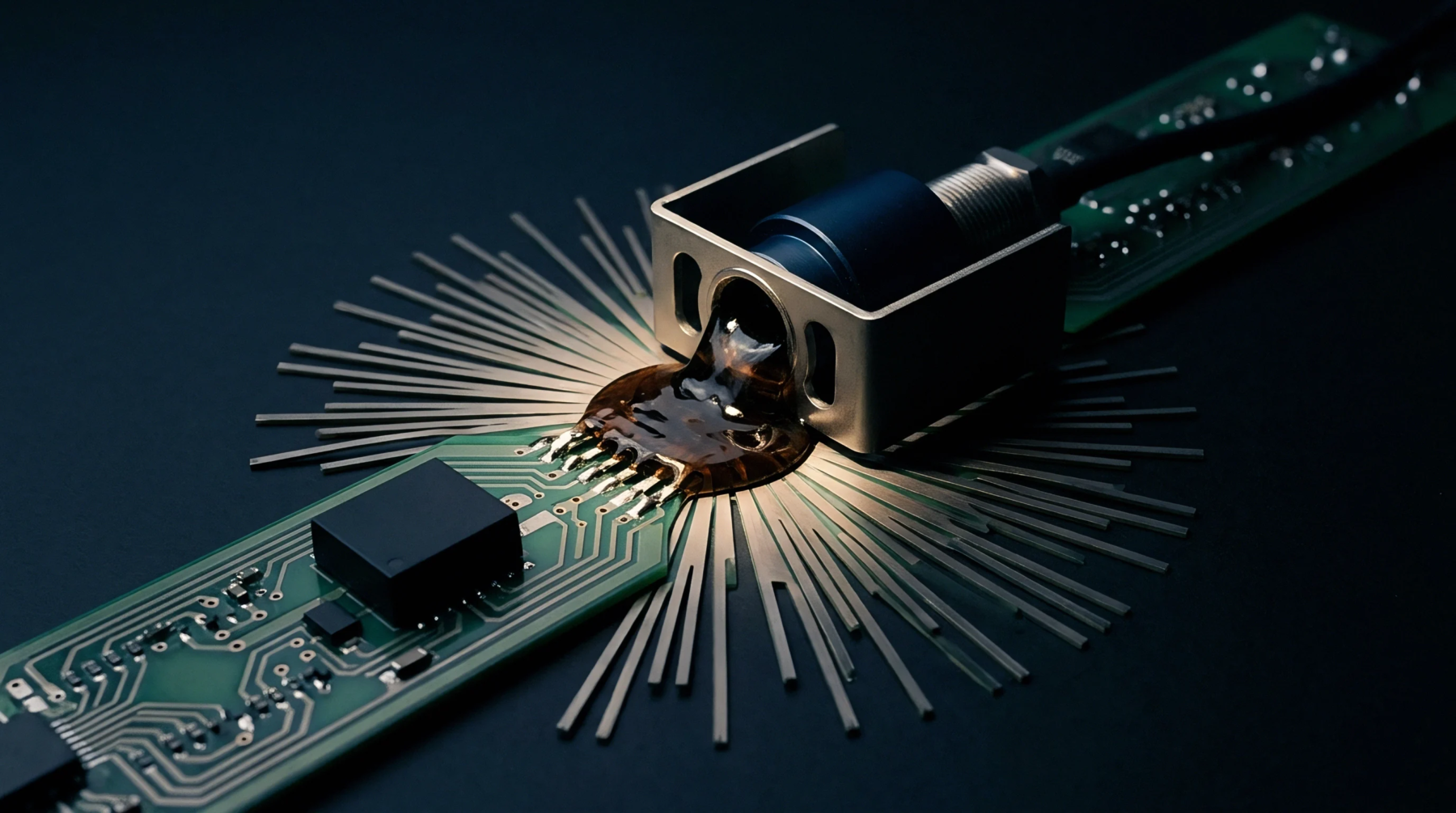
Vacuum lamination compacts copper tooth profiles and redistributes resin fractions, escalating high-frequency insertion loss far beyond datasheet values.
Low-profile copper foils reduce high-frequency conductor loss by minimizing surface roughness path extension, trading signal integrity against peel strength.
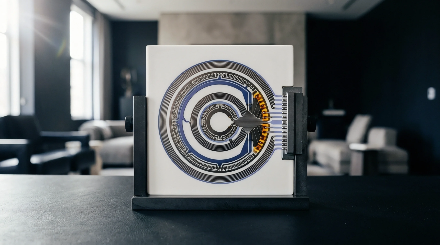
Dielectric relaxation drives high-frequency core attenuation through phase-lagging dipoles, requiring causal modeling and hybrid stackups to balance board costs.

Extracting sub-terahertz dielectric tensors requires combining orthogonal transmission lines with multi-line TRL de-embedding to resolve anisotropic permittivity.
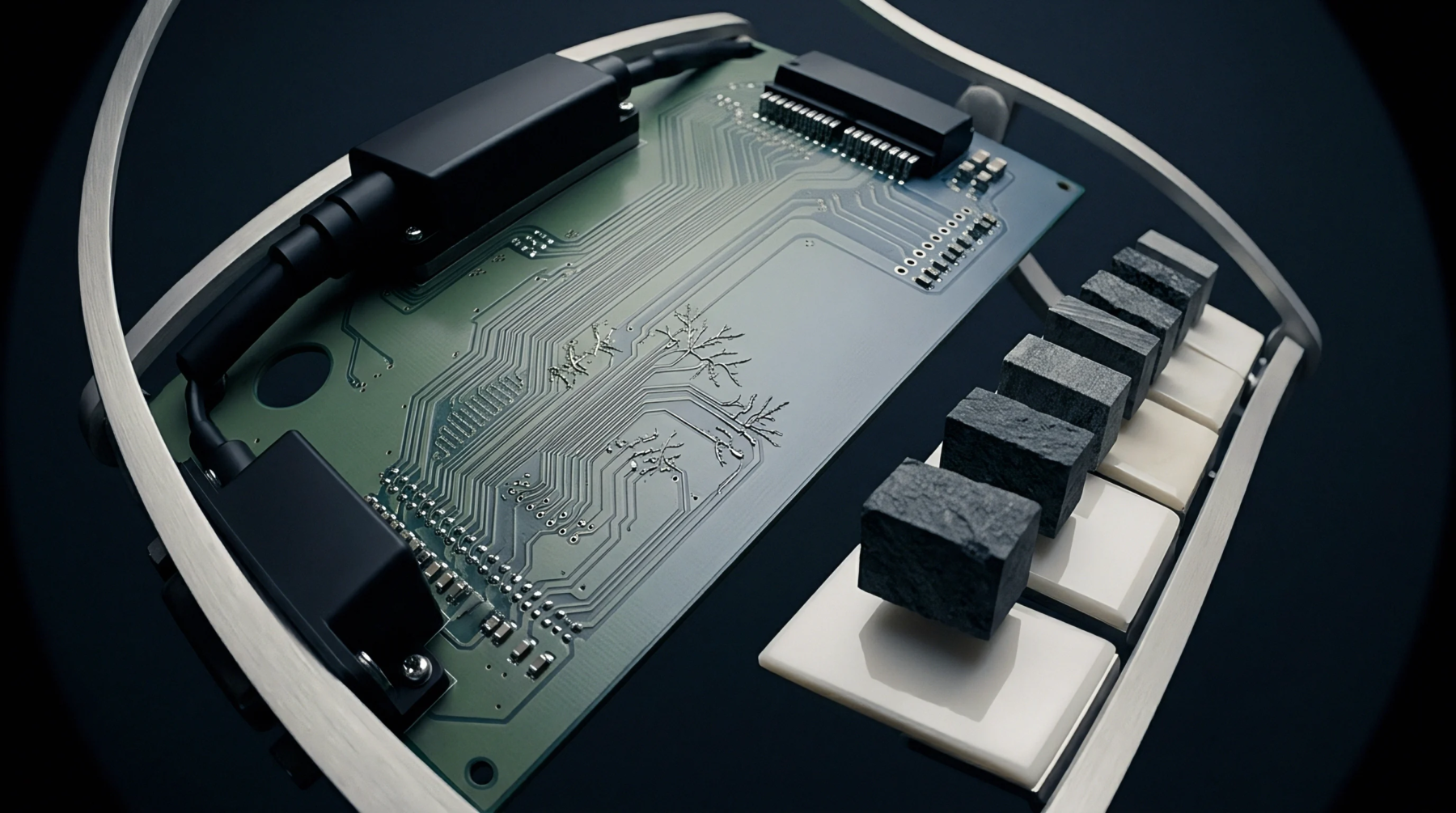
Nanoscale interface texturing eliminates target pad shear delamination in any-layer assemblies by swapping macro-mechanical teeth for molecular silane bonds.
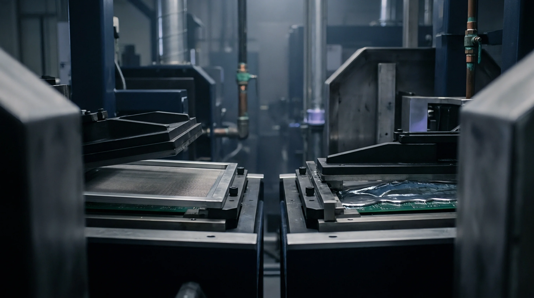
Interfacial bubble nucleation is governed by substrate surface energy and volatile outgassing kinetics, controlling void formation in molten solder joints.
Expertise is a utility, not a secret. sentiention™ publishes its working knowledge as open reference: intelligence layer covering the materials it sources, the markets it enters, and the reference that serves both.