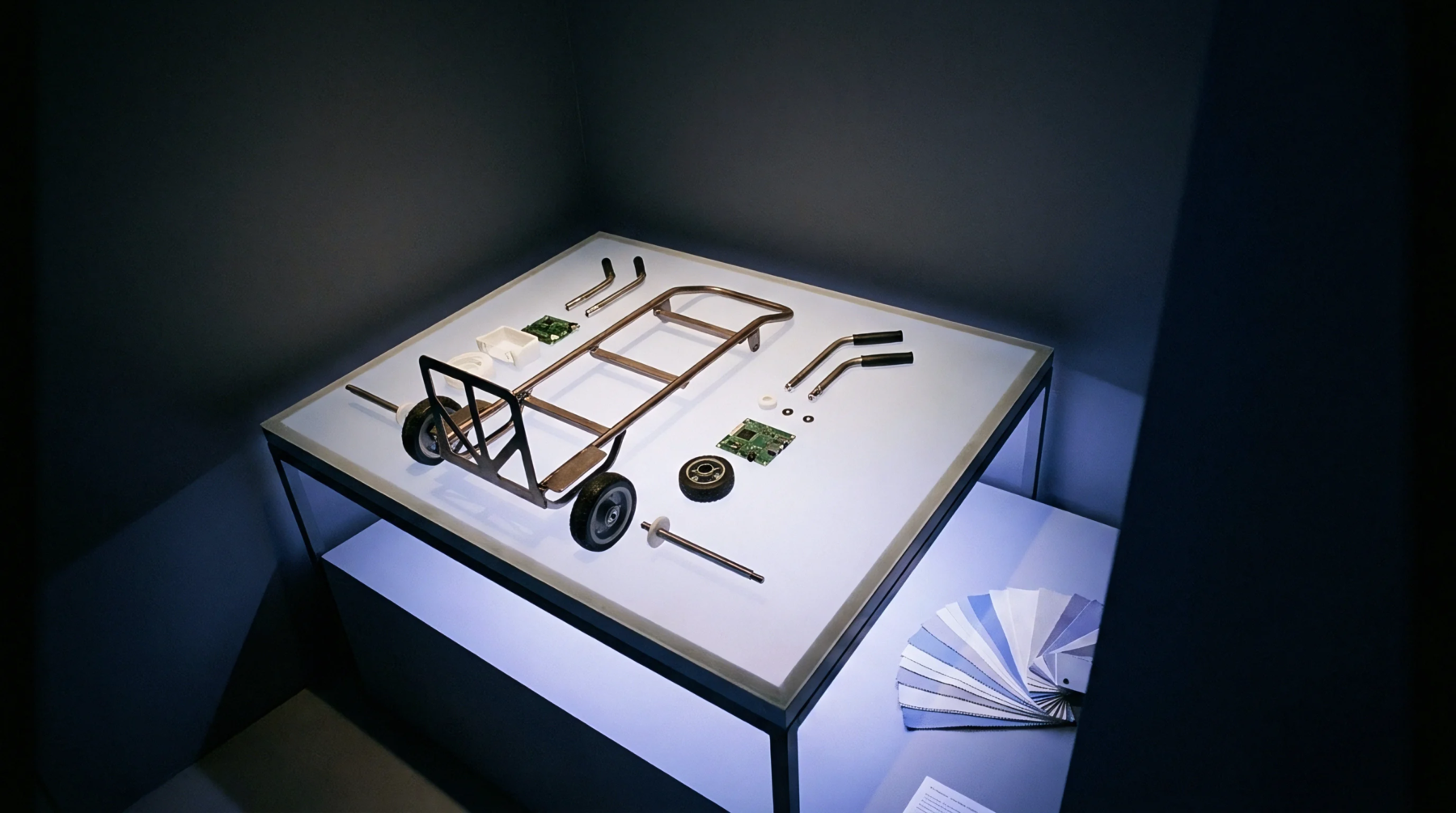
How a Printed Circuit Board Is Built Layer by Layer
Multilayer PCB fabrication laminates etched copper cores and prepreg under heat and vacuum, creating vertical interconnects through precision drilling and copper electroplating.
Multilayer PCB fabrication laminates etched copper cores and prepreg under heat and vacuum, creating vertical interconnects through precision drilling and copper electroplating.
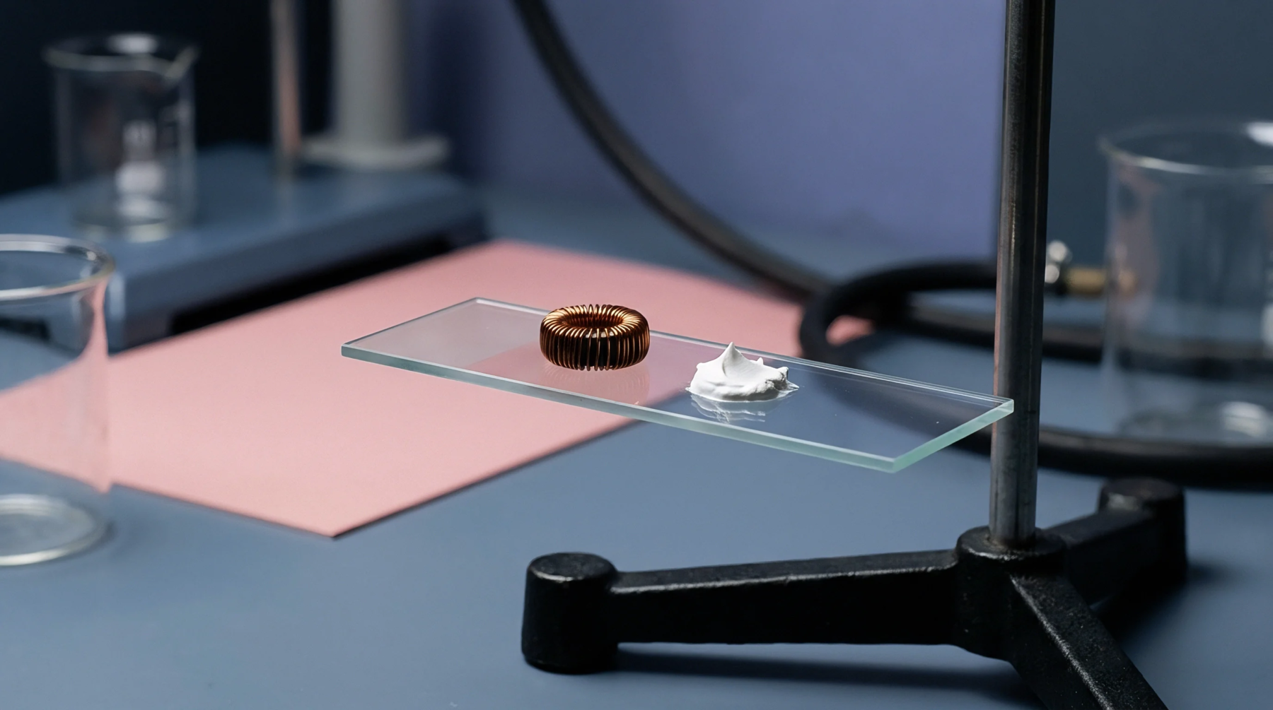
Spread glass weaves minimize micro-spatial permittivity variations, stabilizing high-frequency phase delay when press thermal cycles are tightly controlled.
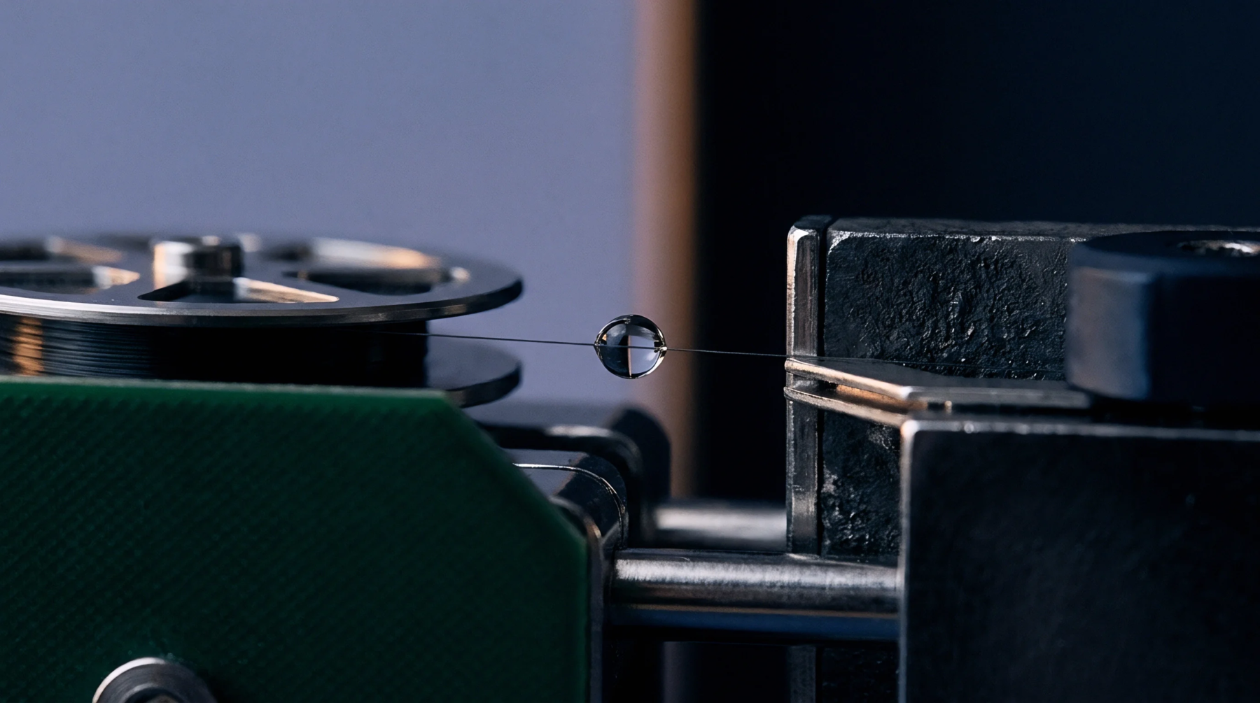
Standard panel coupon architectures must balance border placement against current density gradients to ensure microsections accurately reflect internal board quality.
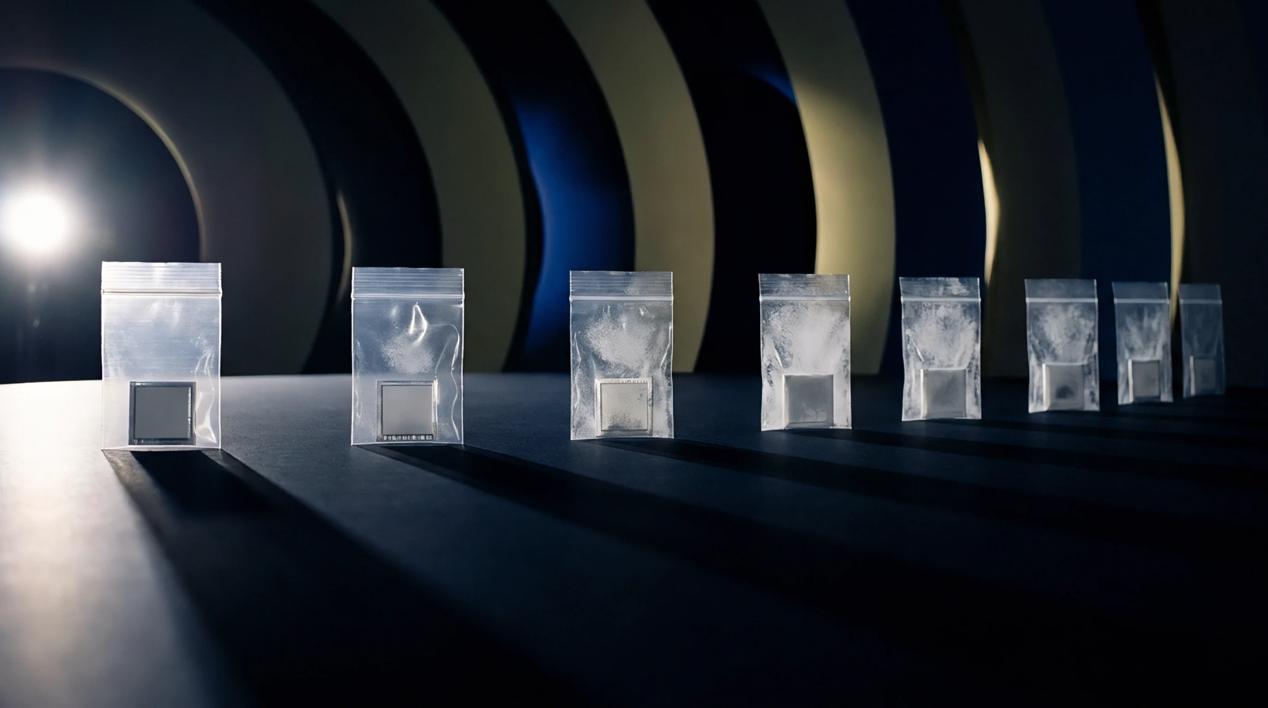
Correlating micro-ohmic resistance drift in thermal stress coupons with microsection defect rates isolates latent inner layer post separation before assembly.

High-frequency laminate rheology dictates prepreg flow kinetics, fixing pressed dielectric thickness, local impedance stability, and panel registration yield.
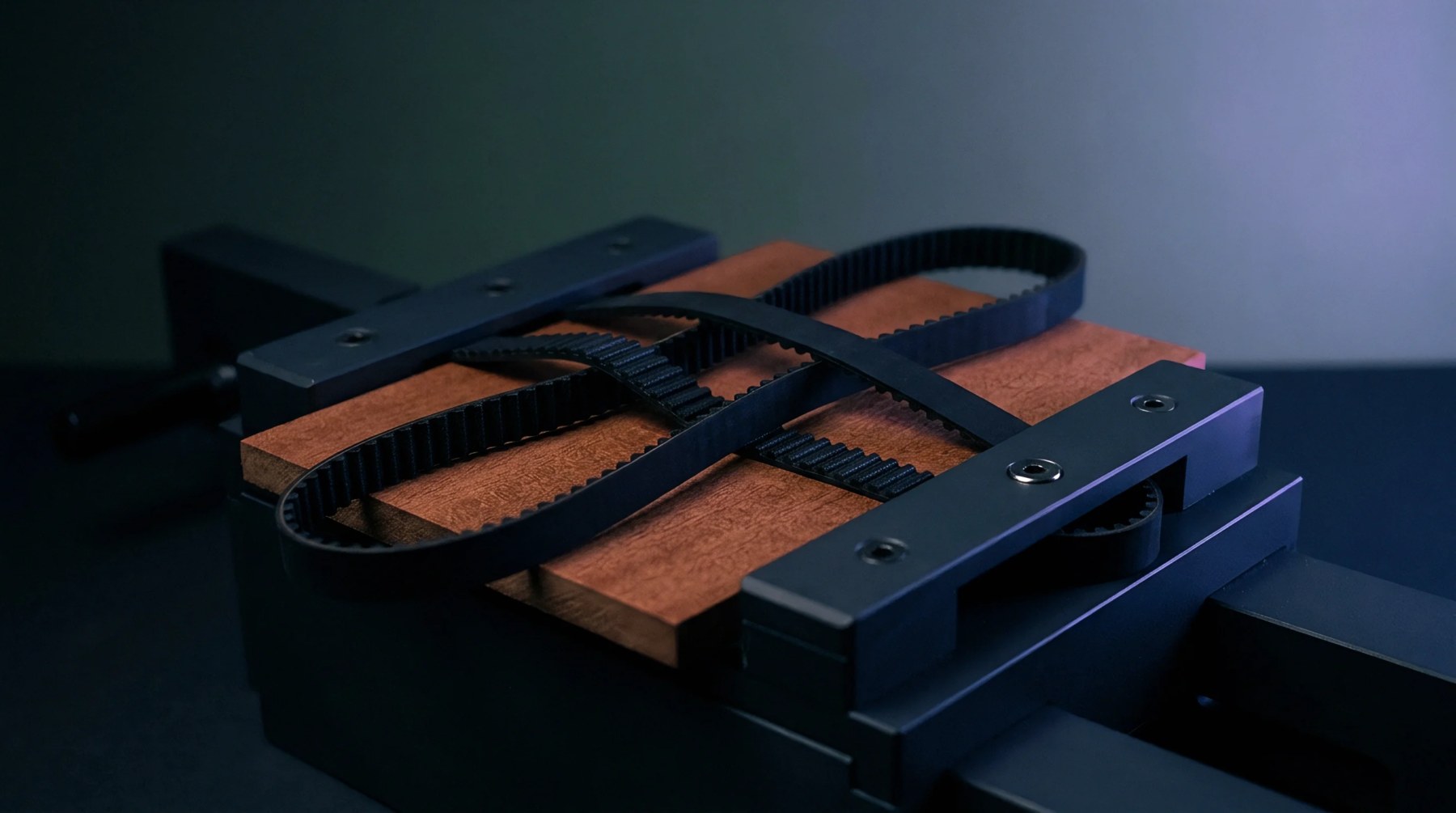
Subassembly press hydraulic parallelism and thermal ramp control determine resin distribution, eliminating dielectric height variation and differential signal phase skew.
Mid-loss laminates optimize high-speed signal reach between 5 and 28 Gbps by controlling dielectric loss without imposing low-loss fluoropolymer costs.
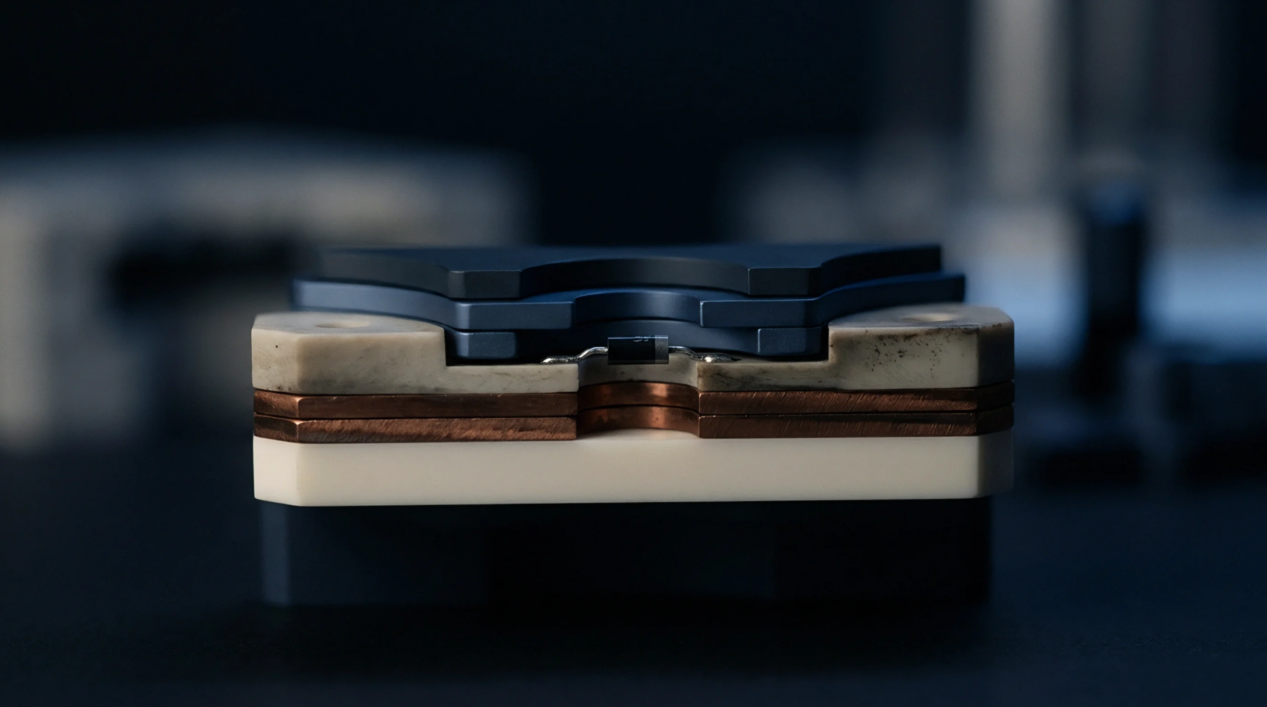
Substrate dielectric drift alters high-frequency signal phase velocity and impedance under thermal stress, requiring flat TCDk resin selection to hold timing margins.
Selecting dielectric substrates requires balancing dissipation factor, glass weave uniformity, foil roughness, and panel yields to meet high-speed impedance targets.
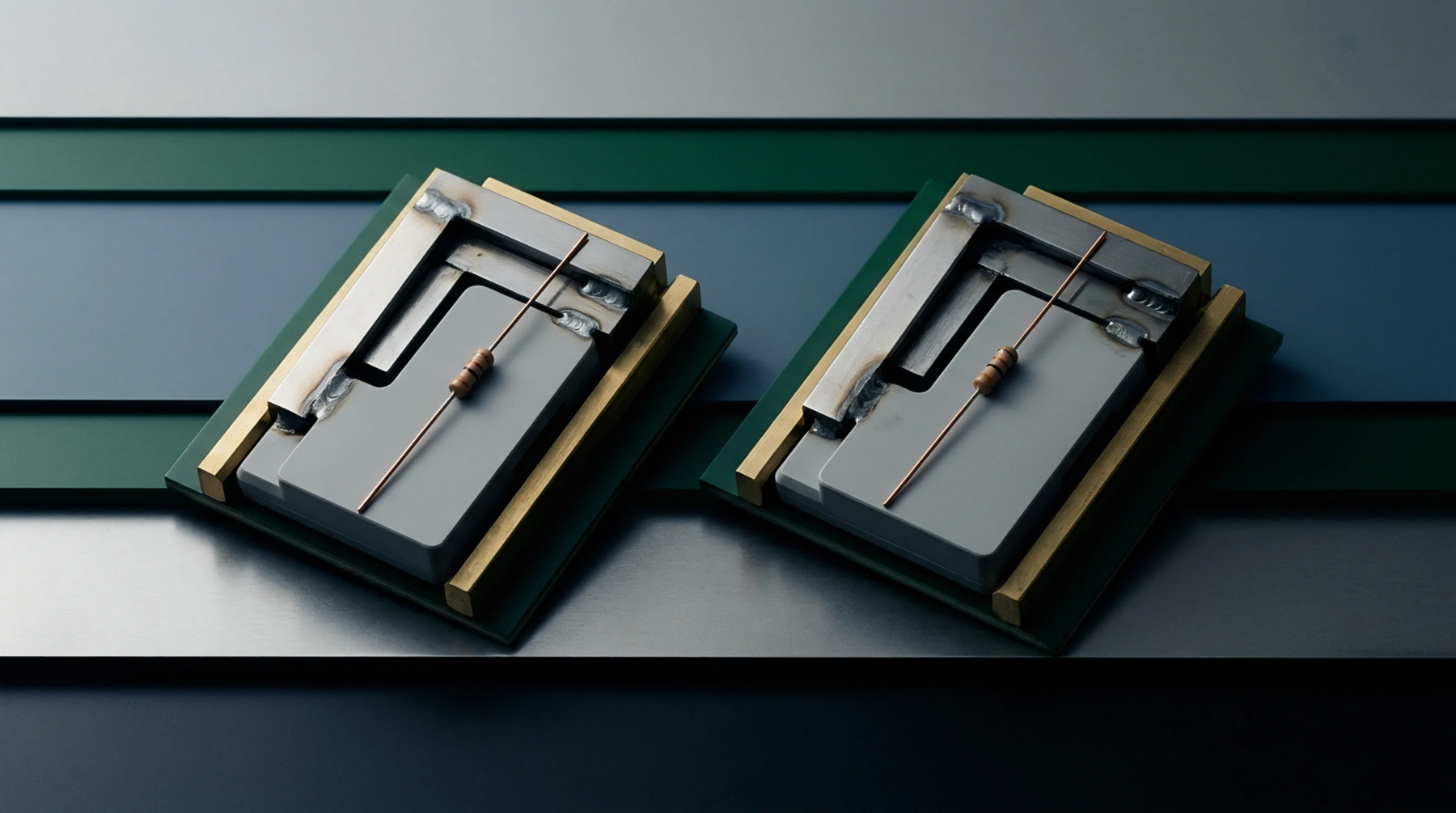
Stackup thickness control requires calculating pressed prepreg heights over local copper patterns to hold impedance and microvia drilling tolerances.
IPC-4101 slash sheets establish mandatory baseline physical, thermal, and electrical limits that override generic trade names to enforce material reliability.
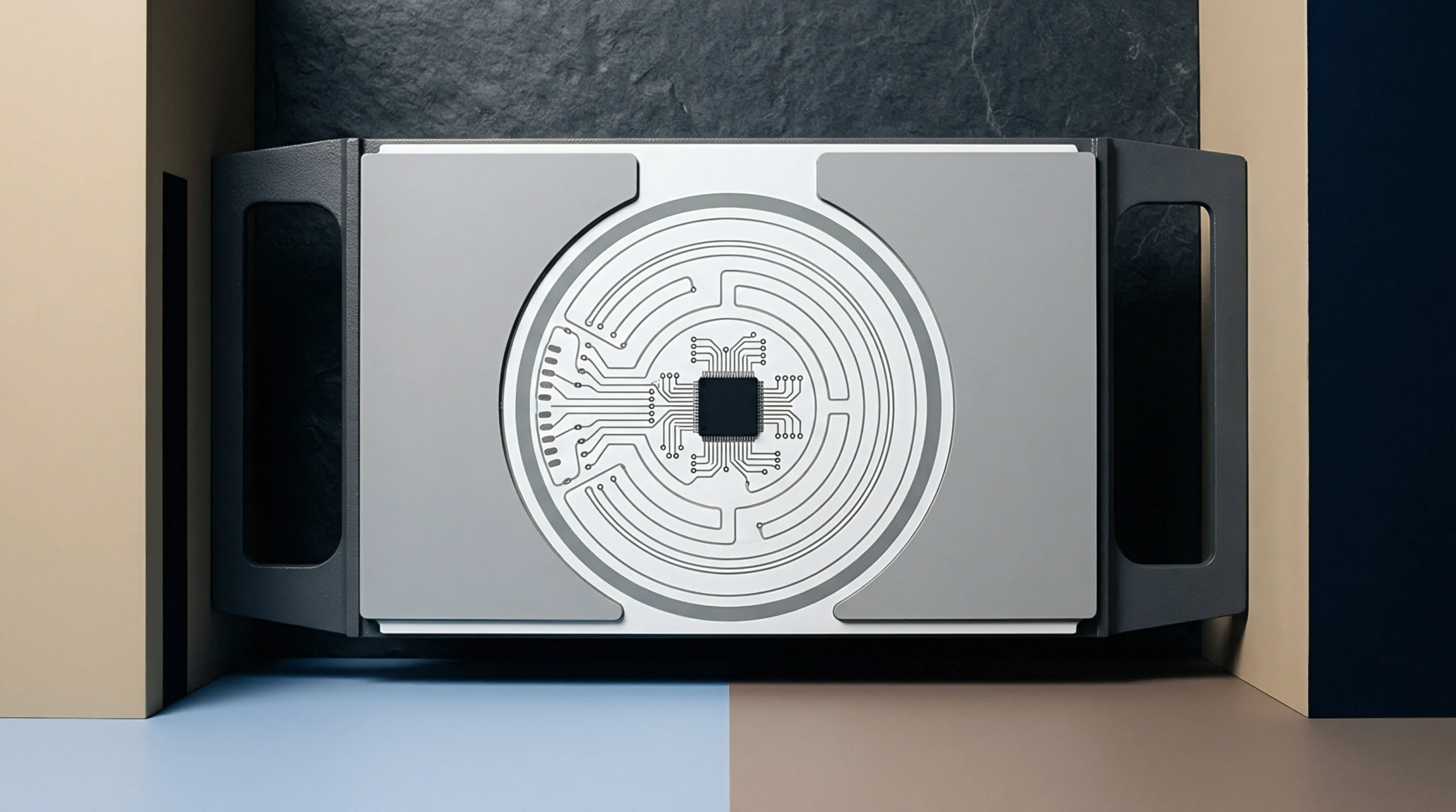
Sequential lamination induces non-linear dielectric relaxation at glass-resin interfaces, shifting Dk up to 0.14 and altering impedance by over 4 ohms.
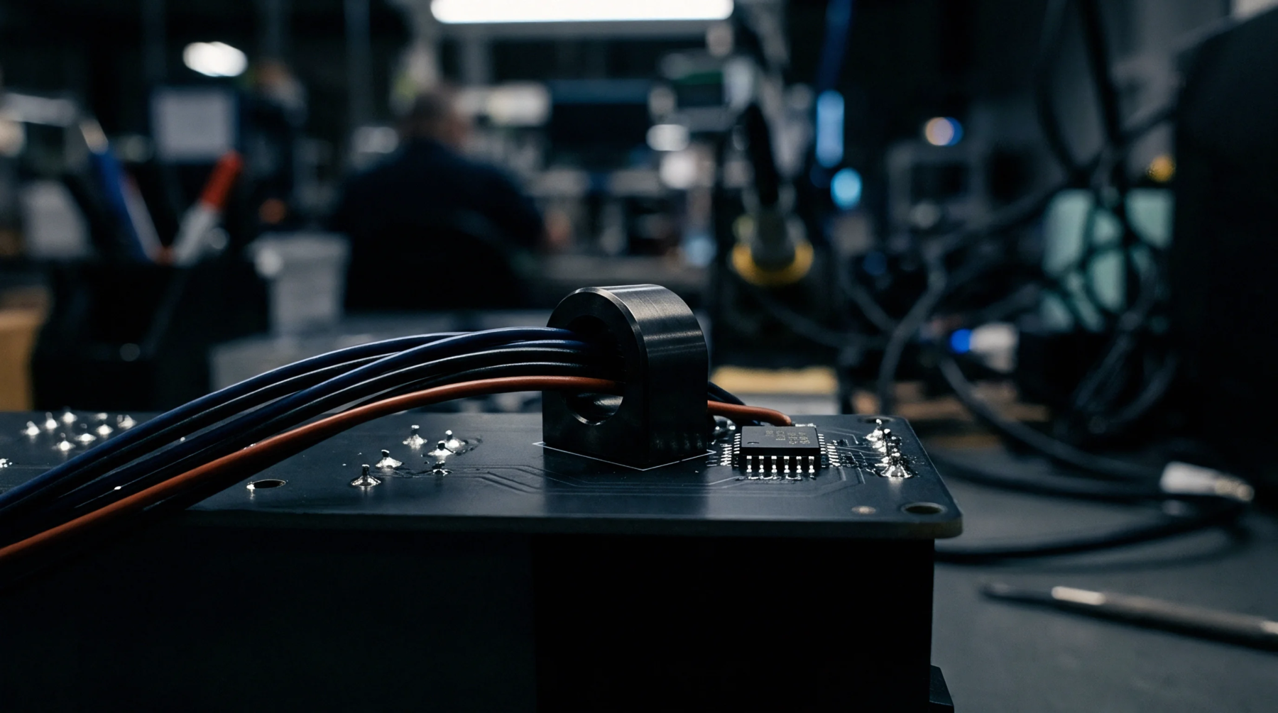
Mitigate sub-core microvia target pad delamination by enforcing eighteen-micrometre foils, controlled microetching, and staggered layout architectures.

Anisotropic tensor creep models prevent layer misregistration and microvia failure by accounting for glass weave shear strain under reflow thermal cycles.
Capture pad size equals laser diameter plus twice the root-sum-square of tool, drill, and lamination movement tolerances.

Dynamic prepreg viscosity and cure kinetics dictate resin flow windows, microvia filling completeness, and layer encapsulation during HDI board lamination.
Sub-tier material drift erodes high-reliability board margins; mathematical risk modeling and rigorous chemical dossier validation eliminate latent field escapes.
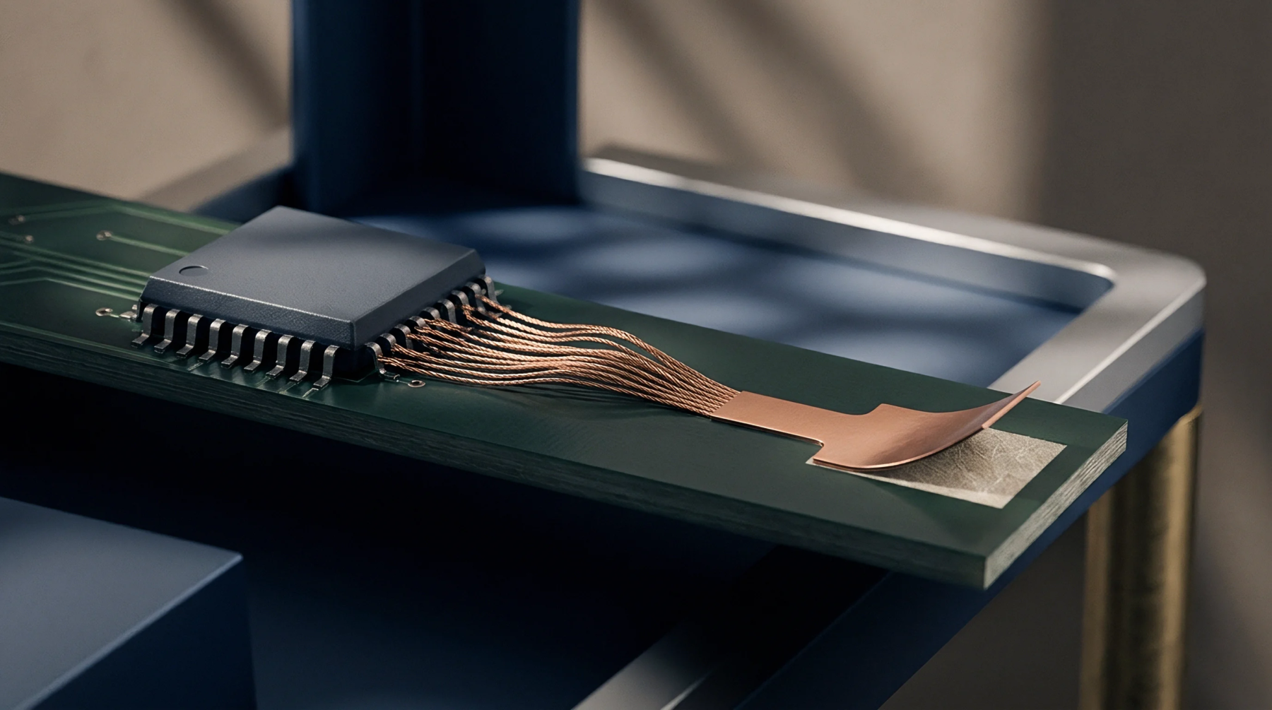
Optimizing rigid-flex stackups for high-speed signals requires adhesiveless polyimide cores, cross-hatched reference alignment, and staggered rigid transitions.
Thermal cycles in high density stackups drive copper recrystallization, causing grain growth and vacancy coalescence that trigger microvia interface failures.
Optimizing plasma desmear for heterogeneous laminates balances differential etch rates across polymer chemistries to ensure plating adhesion without wedge defects.
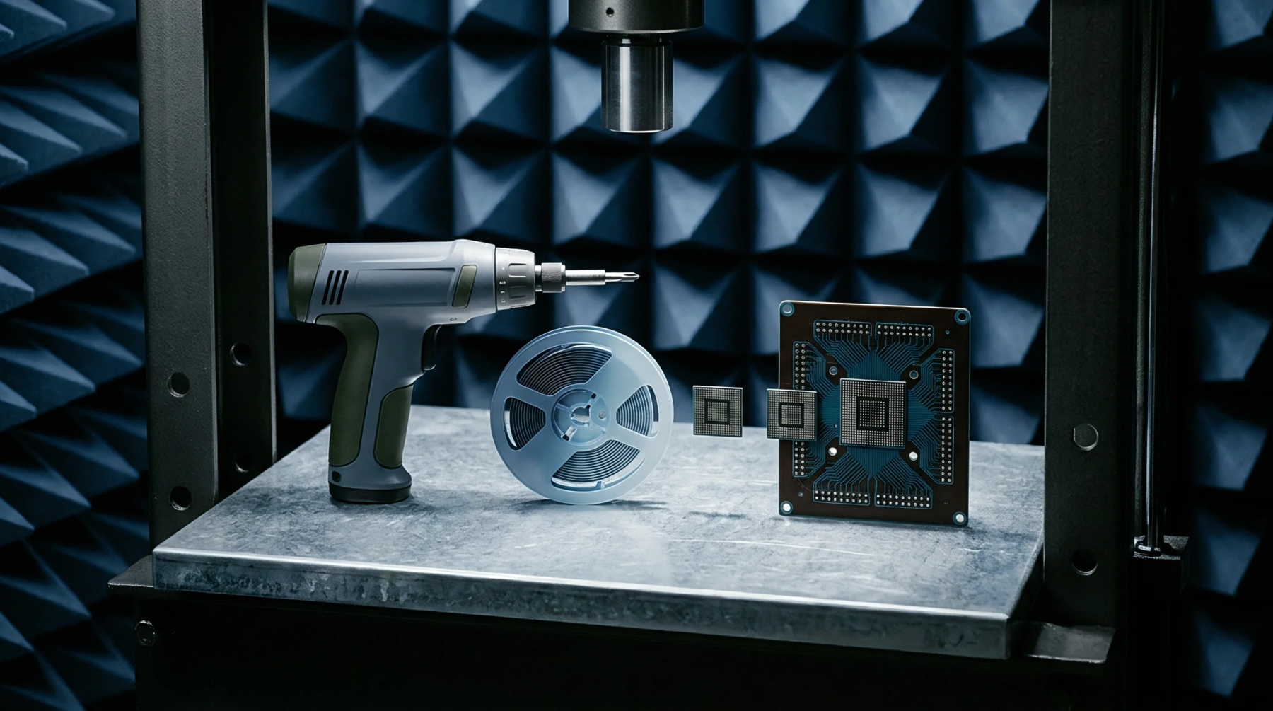
Asymmetric ultra-low-loss stackups shift the neutral axis and concentrate reflow shear strain at copper boundaries, requiring aspect ratios under 10:1 to protect barrel fatigue life.
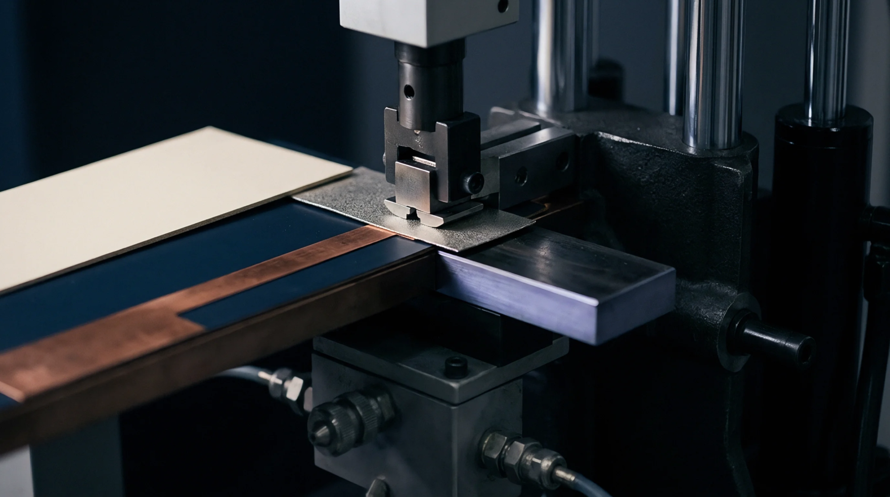
Optimizing inner layer copper thickness and prepreg fill demands matching matrix resin volume to clearance void area while controlling pressed dielectric height.
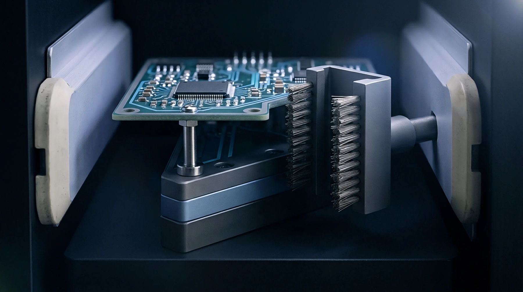
Z-axis laminate expansion exceeding copper ductility during lead-free reflow drives microvia failure, requiring high-Tg filled dielectrics and coupon screening.
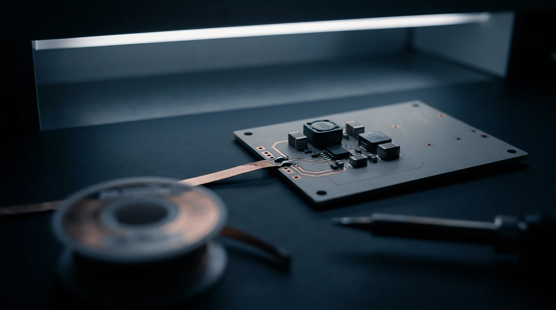
Weibull shape and location parameters derived from microsections quantify true target pad clearance safety margins, protecting buyers from latent dielectric field failures.
Hybrid multilayer selection pairs low-loss RF laminates with epoxy bases by matching cure windows, controlling z-axis expansion, and optimizing panel yields.
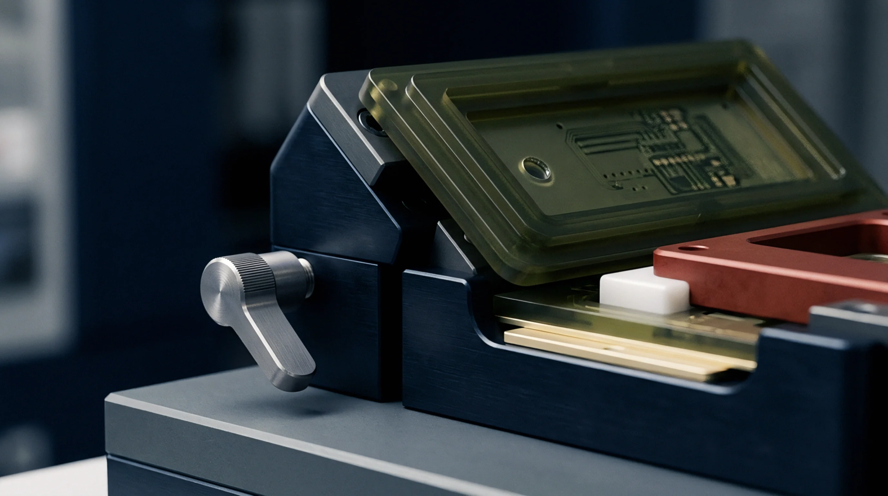
Optimizing inner layer copper balance balances z-axis stress across the stackup, suppressing bow and twist to ensure high-yield SMT component placement.
Spread glass prepreg flattens yarn bundles to eliminate local resin windows, cutting differential skew without the severe panel waste of rotated artwork.
IPC-4101 slash sheets classify base laminate properties to bind fabricators to verifiable resin, thermal, and electrical limits on production drawings.
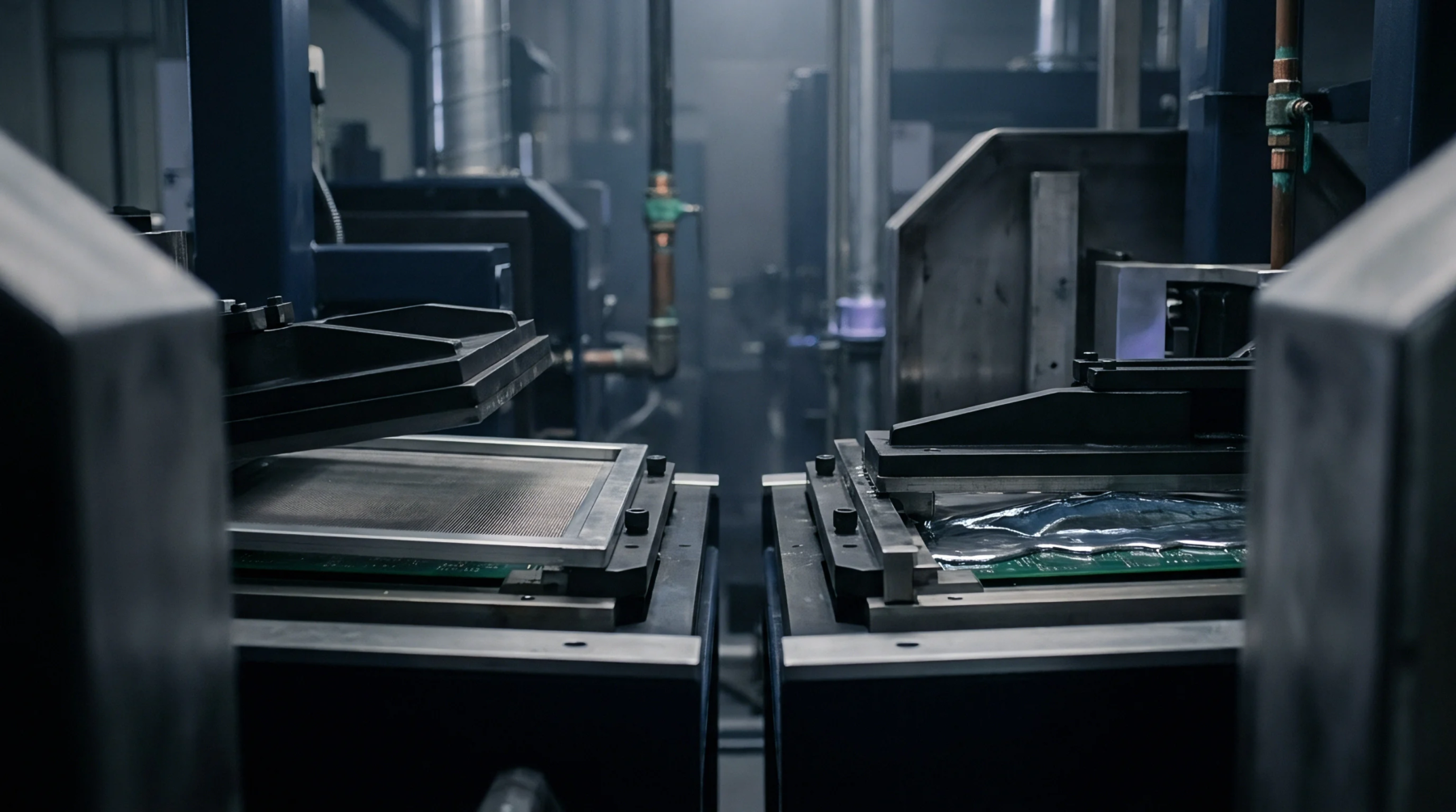
High-frequency laminate selection for lead-free assembly requires low z-axis expansion and high decomposition temperatures to survive 260°C reflow stresses.
Environmental temperature and humidity cycling degrades substrate integrated waveguide cavity damping by elevating loss tangents and fracturing via fences.
Expertise is a utility, not a secret. sentiention™ publishes its working knowledge as open reference: intelligence layer covering the materials it sources, the markets it enters, and the reference that serves both.