
In Circuit Test Fixture Strain Gauge Commissioning and Deflection Verification
Commissioning in-circuit test fixtures with triaxial strain gauge rosettes per IPC/JEDEC-9704A prevents test-induced solder joint and pad cratering failures.
Commissioning in-circuit test fixtures with triaxial strain gauge rosettes per IPC/JEDEC-9704A prevents test-induced solder joint and pad cratering failures.

SMT setup delays, component scrap overages, and rework thermal damage are governed by explicit contractual downtime tariffs, material allowances, and IPC inspection limits.

Unambiguous contract allocation caps assembly liability at process fees while tying thermal damage claims to independent coupon microsectioning evidence.

Thermal defect attribution in mixed consigned assembly requires combining profile logs, 3D X-ray data, and MSL handling records to split material and process liability.

Test point geometry and access density directly dictate structural fault coverage, fixture expense, signal integrity, and field escape liabilities across production batches.

Bed-of-nails test fixtures demand empirical strain gauge verification to ensure dynamic microstrain levels stay below component limits and prevent latent pad cratering.

Allocating latent defect risk in advanced assembly relies on defined screening limits, clear warranty triggers, and empirical root-cause testing formulas.

Boundary scan TAP probe evaluation demands dynamic contact resistance monitoring under 20mV dry-circuit limits to prevent false structural defect calls.

Integrating IEEE 1149.1 boundary scan with flying probe target vectors maximizes fault coverage on high-density PCBs while slashing test times and fixture costs.

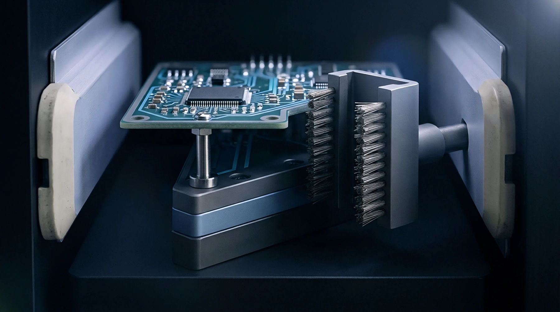
Balancing micro-probe forces with precision push-fingers prevents substrate strain over 500 microstrain, protecting fine-pitch BGAs and MLCCs from fixture damage.

Allocate micro BGA line standby and rework exposure by binding hourly downtime tariffs and hot-gas rework liability directly to SPI, AXI, and feeder logs.

Cyanate ester flexural stiffness induces adhesive shear lag and interfacial microcracking, causing rosette signal loss and latent solder interconnect escapes.

Attributing intermittent BGA escapes requires pairing boundary scan fault coverage metrics with calibrated nanosecond discontinuity logging during line audits.
Optimized lead-free reflow profiling requires thermal deltas under eight degrees, controlled time above liquidus, and precise paste transfer efficiency.

Combining IEEE 1149.6 boundary scan vectors with deflection-assisted flying Kelvin probes isolates unmasked BGA head-in-pillow defects down to 4.5 micro-ohms.

AC coupling capacitor solder joint failures require AC boundary scan and TDR screening to detect latent mechanical microcracks before field deployment.
Microvoid coalescence under thermal cyclic strain stems from creep-fatigue interaction at intermetallic layers, requiring EBSD and strain partitioning to prove.

Controlling internal deposit stress below 150 MPa tensile in nano-crystalline nickel plating prevents cyclic microstructural relaxation and joint fracture.
Substrate thermal distortion stems from CTE mismatch and copper asymmetry, requiring tight dynamic warpage limits and carrier tooling to protect joint yield.

Quantifying dynamic strain gradients and rate-dependent tensile limits around dense BGA corners prevents latent dielectric pad cratering during assembly.

Minimizing ICT solder joint fatigue requires triaxial strain gauge profiling below 500 microstrain at actuation speeds under 1,000 microstrain per second.

IPC JEDEC 9704 strain measurement protects PCB assemblies by quantifying dynamic handling stresses to prevent BGA solder joint cracking and pad cratering defects.
Z-axis laminate expansion exceeding copper ductility during lead-free reflow drives microvia failure, requiring high-Tg filled dielectrics and coupon screening.

Establishing quantitative strain rate envelopes prevents intermetallic cleavage and pad cratering in lead-free circuit assemblies during manufacturing.

Triaxial rosettes placed adjacent to component corners capture multi-axis dynamic strain and strain-rate spikes, preventing latent solder interconnect fracture.
Dynamic strain rate transformation during fixture actuation verifies mechanical compliance against IPC-9704 limits before structural testing begins.
Hybrid multilayer selection pairs low-loss RF laminates with epoxy bases by matching cure windows, controlling z-axis expansion, and optimizing panel yields.

Contractual recovery for intermittent SMT failures requires 3D SPI volume logs, dynamic thermal profiles, and certified SEM intermetallic microsections.

Non-redundant aggregation of optical, X-ray, and boundary scan coverage metrics determines true defect escape risk on high-density circuit boards.
Flying probe capacitance screening locates open nets rapidly, while four-wire Kelvin micro-ohm verification isolates hidden trace necking and micro-via cracks.
Expertise is a utility, not a secret. sentiention™ publishes its working knowledge as open reference: intelligence layer covering the materials it sources, the markets it enters, and the reference that serves both.