
Controlling Resin Rheology during Multi Cycle Sequential Lamination Press Runs
Synchronizing temperature ramp rates with hydraulic pressure setpoints maintains minimum resin viscosity windows and prevents sequential lamination voiding.

Synchronizing temperature ramp rates with hydraulic pressure setpoints maintains minimum resin viscosity windows and prevents sequential lamination voiding.
Glass bundle heterogeneity induces differential phase skew that requires spread cloth styles, trace angling, or low-Dk glass to maintain channel eye closure.

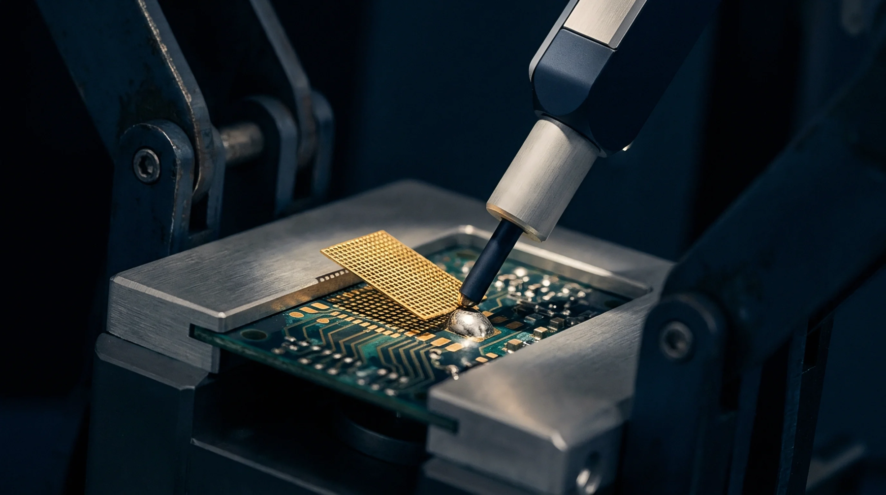
Titanium inserted pallet apertures isolate fine pitch connector pins with 0.4mm walls that prevent composite erosion, bridging, and thermal sink defects.
Aspect ratios below 0.55 require electroformed or nanocoated foils and slow separation speeds below 0.2 mm/s to prevent wall friction starving solder deposits.

Calibrated broad ion beam cross-sectional electron microscopy arbitrates fine-line etch disputes by eliminating mechanical smear and edge blooming errors.

Type 5 solder pastes lower practical stencil area ratio limits from 0.66 down to 0.45 when paired with nanocoated or electroformed foils.

Flash etch undercut in fine line substrates requires multi-angle AOI and referee cross-section SEM to catch base copper loss hidden beneath nominal trace crowns.
Evaluating solder paste volume across fine pitch pads requires maintaining area ratios above 0.55 and enforcing 3D inspection windows between 75 and 120 percent.

Ultra-thin seed layer failure stems from CTE-driven interfacial shear and barrier oxidation, mitigated by coupon-verified peel retention after 260°C reflow.
Electroless copper seed thickness variations widen flash etching dwell times, causing severe lateral undercut, collapsed etch factors, and impedance scrap.

Automated cross-tier notification ingest links component delta qualification directly to technical file updates to prevent regulatory seizure and field failures.

Active technical file maintenance binds physical circuit components to traceable test evidence, preventing customs seizures and sales bans under EU surveillance.

Rigorous verification of PCBA artwork, BOM netlists, and compliance dossiers before release prevents receiving holds, line downtime, and field returns.

Modeling AC-coupled scan channels requires combining IEEE 1149.6 low-frequency pulse decay with microwave pad parasitics to stop latent defect escapes.
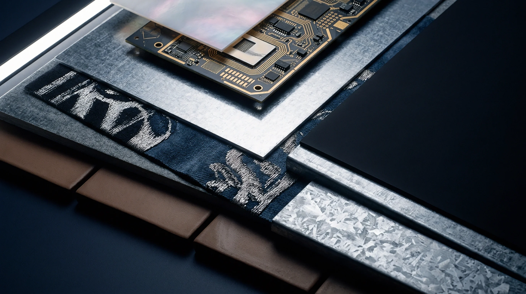
Weighted fault coverage balances boundary register access against unmonitored cluster pins to calculate genuine manufacturing defect escape risk.

Oblique radiographic spatial calibration ties projection matrices to physical phantoms, preventing non-isomorphic voxel blur from distorting SMT void metrics.

Dynamic multi-sensor thermal stage compensation maintains sub-micron inspection accuracy, preventing false solder joint defect calls on advanced packaging lines.

Hybrid fixture nodal access limits depend on probe pointing accuracy, PCB flexure under IPC-JEDEC-9704 strain limits, and boundary scan partitioning.

Fine line HDI etching yield hinges on managing lateral undercut through thin copper foils, uniform fluid spray dynamics, and semi-additive process transitions.

Staggering microvias dissipates out-of-plane laminate thermal expansion through trace bending, reducing reflow interface stress by more than forty percent.
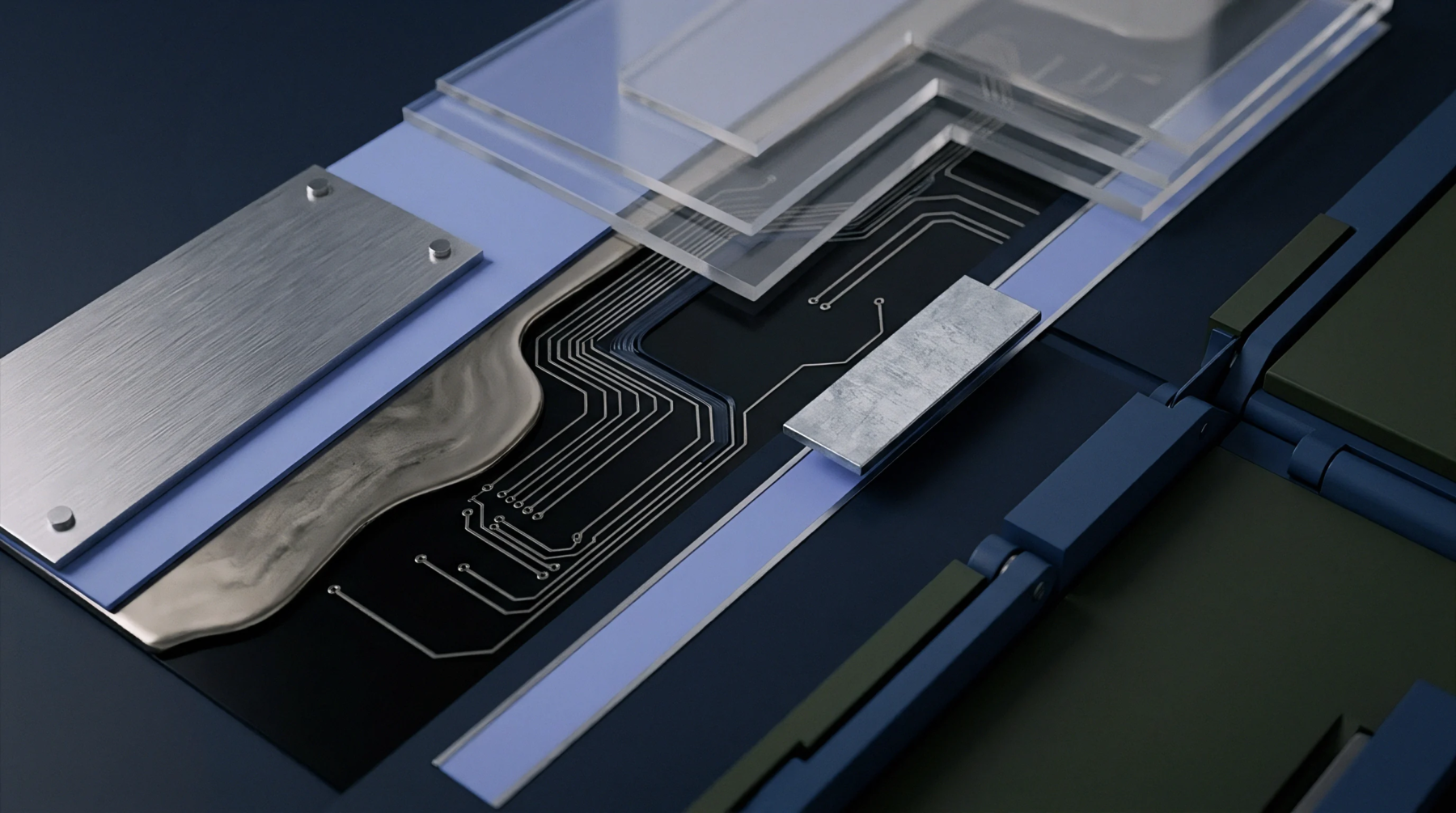
Bottom-up microvia superfilling requires suppressing surface deposition while accelerating via base plating via strict boundary layer and additive controls.
X-ray spatial magnification depends on source-to-object geometry; uncorrected thermal stage drift causes measurement errors that compromise solder joint qualification.

Maintain microvia aspect ratios below 0.75:1 using thin dielectrics to secure void-free copper plating and survive multi-cycle lead-free assembly reflow.
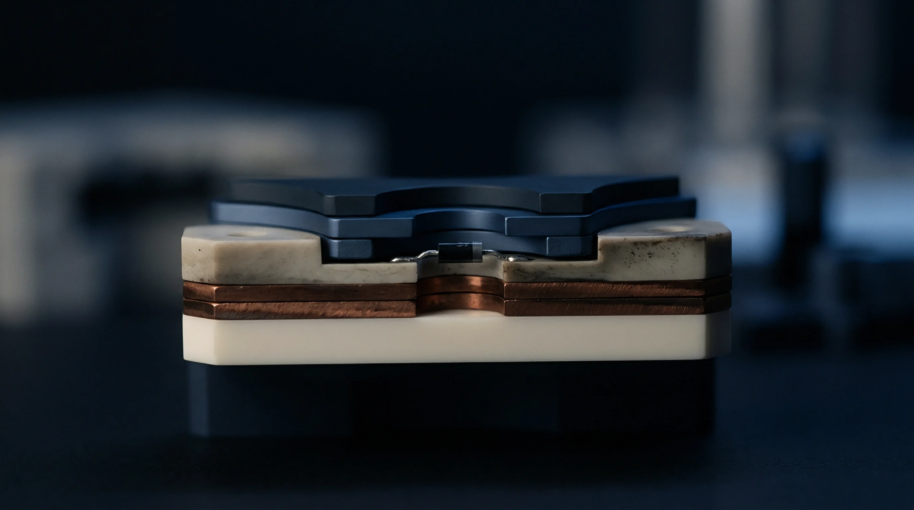
Thermal cycling in multi-stage rigid-flex presses collapses free volume and elevates dielectric constant, requiring scaled artwork to maintain impedance tolerances.

Real-time thermal gradient control and tuned peel-off dynamics secure Class 3 vertical hole fill while preventing bridges and copper knee dissolution.

Verify AC boundary scan using IEEE 1149.6 pulse and train routines under stress screening to stop high-speed structural solder escapes before product delivery.
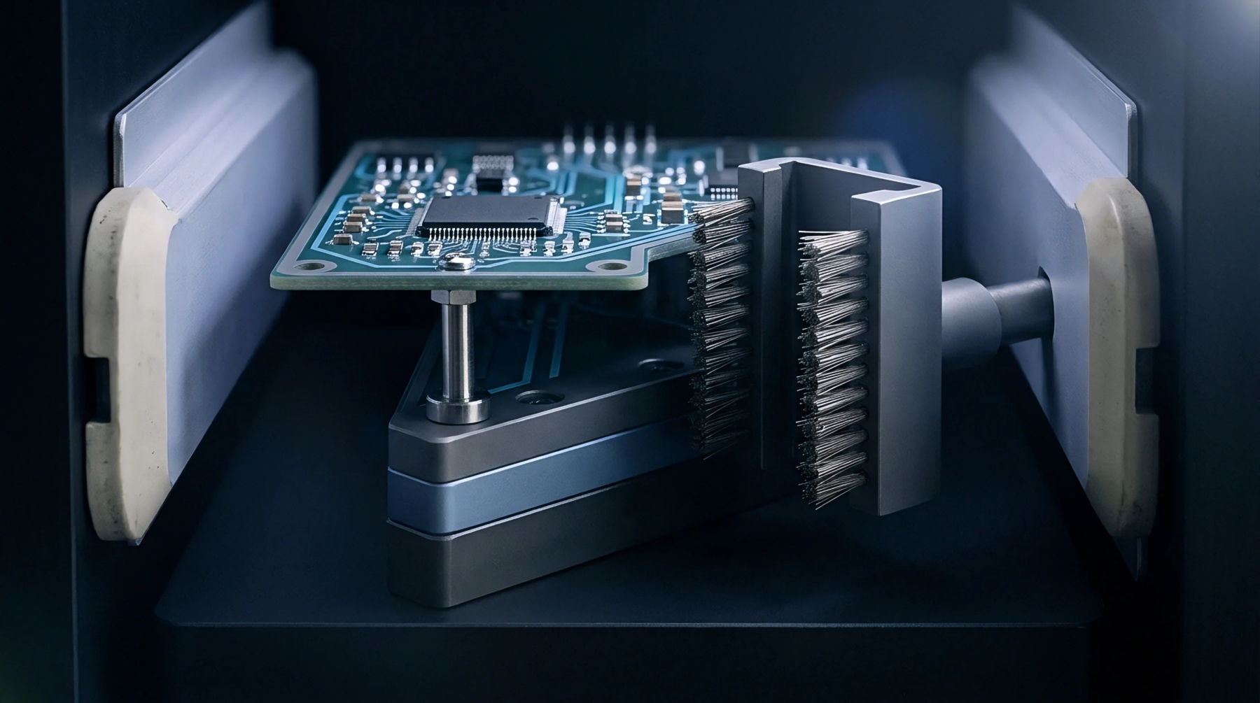
Integrating boundary scan files into in-circuit fixtures reclaims blind BGA net coverage, cuts mechanical probe force, and lowers board diagnostic debug costs.

Holding top-side preheat between 105 C and 130 C prevents inner-plane solder freezing, securing complete through-hole fill without secondary reflow.
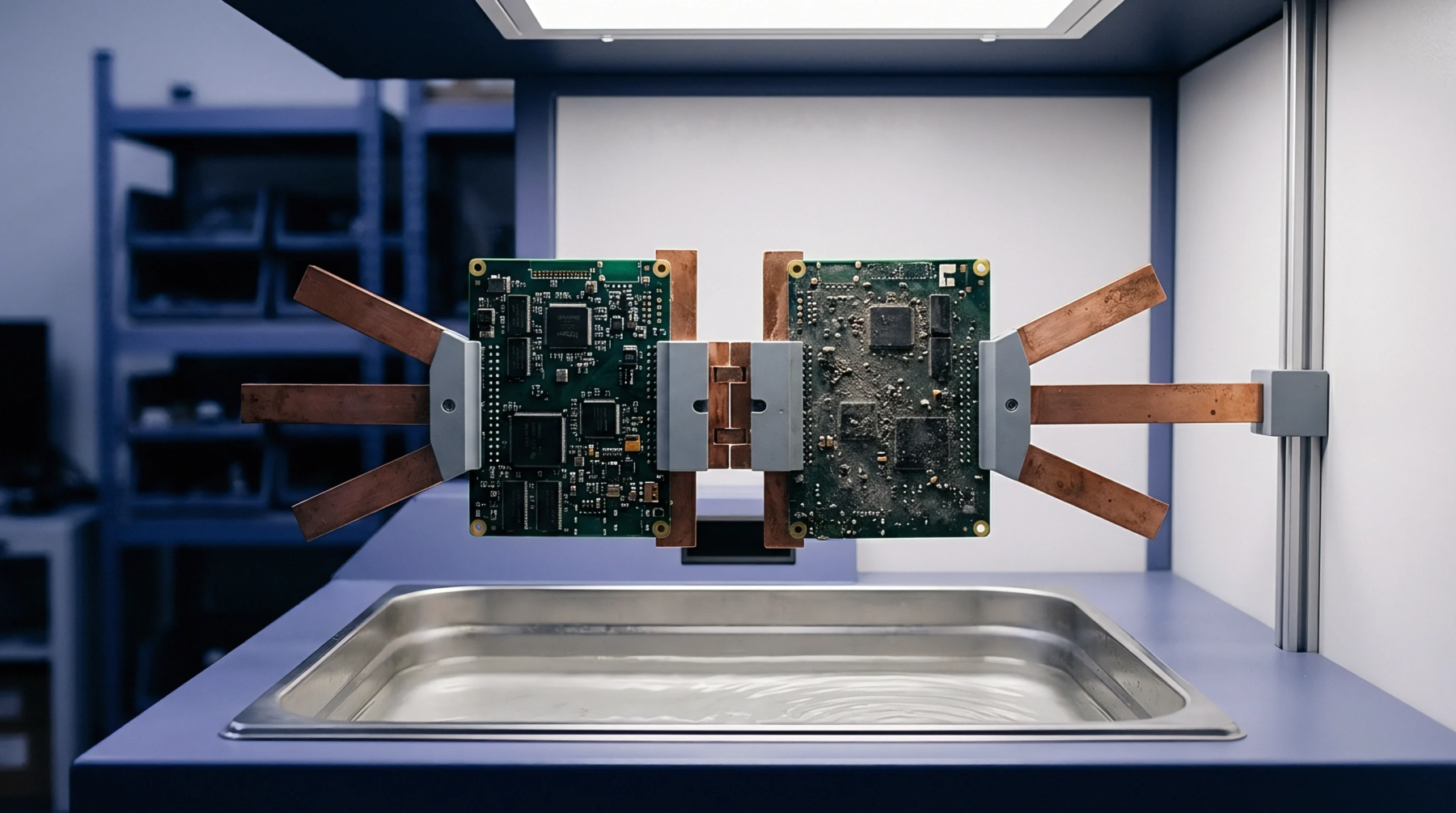
Configure clean TAP terminations, verify BSDL instruction registers, and execute EXTEST vectors to isolate physical solder bridges and open joints.
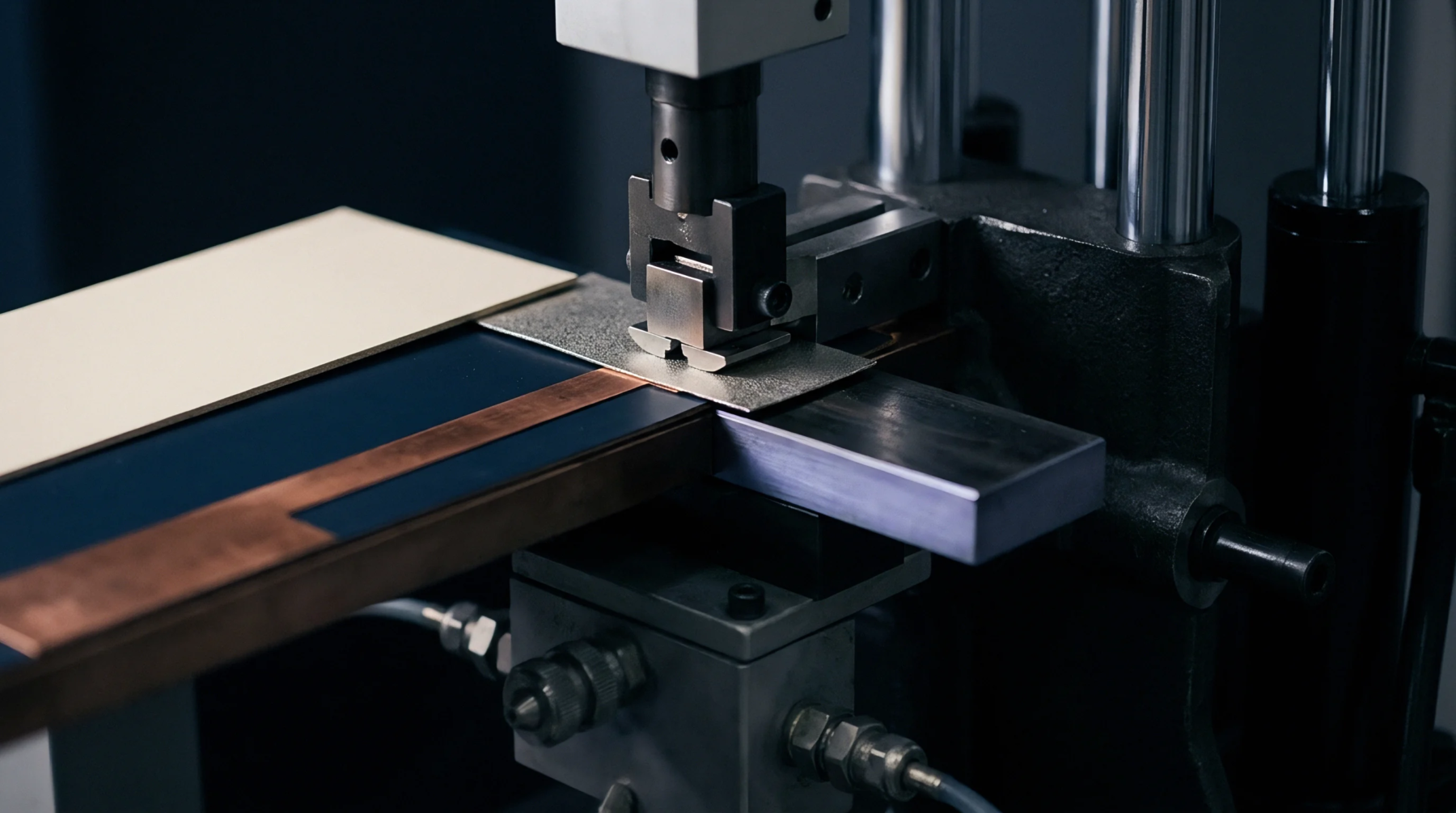
Wettable nozzle selective assembly anchors the solder wave via capillary forces, demanding precise peel speeds and inerting to stop bridging and erosion.
Expertise is a utility, not a secret. sentiention™ publishes its working knowledge as open reference: intelligence layer covering the materials it sources, the markets it enters, and the reference that serves both.