Finite Element Modeling of Ultra-Fast Thermal Ramp Shear Kinetics in PTFE Substrates
Finite element modeling of ultra-fast ramps predicts interfacial shear failure, establishing safe thermal profile limits for high-frequency PTFE circuit boards.

Finite element modeling of ultra-fast ramps predicts interfacial shear failure, establishing safe thermal profile limits for high-frequency PTFE circuit boards.

Convective heat transfer coefficients govern component heating rates and solder joint temperature deltas across circuit boards during forced convection reflow.

Vacuum-assisted reflow with segmented stencil apertures controls voiding below 15 percent on heavy copper assemblies while rigid carrier pallets limit transient z-axis distortion.

Calibrating thermal profiles for asymmetric heavy copper SMT requires extending preheat soak to flatten board delta T before liquidus.
Continuous nanosecond event detection under dry-circuit limits catches contact fretting and joint micro-cracking that slip past standard continuity meters.
Calibrating reflow profiles for heavy copper circuits requires lengthening soak times to collapse thermal deltas across variable mass areas.

Latent substrate microcracks close elastically at room temperature, escaping DC continuity tests until thermal expansion separates the fractured interfaces.

Extended selective soldering dwell drives polycarboxylic acid hydrolysis of silane bonds, accelerating interfacial crack growth along glass fiber bundles.
Controlled preheat soaking between 130°C and 160°C suppresses matrix hydrolysis by volatilizing absorbed moisture before organic acid activators dissociate.

Registration drift compresses inner-layer clearances, converting nominal spacing into steep electric fields that accelerate dielectric rupture and filament growth.
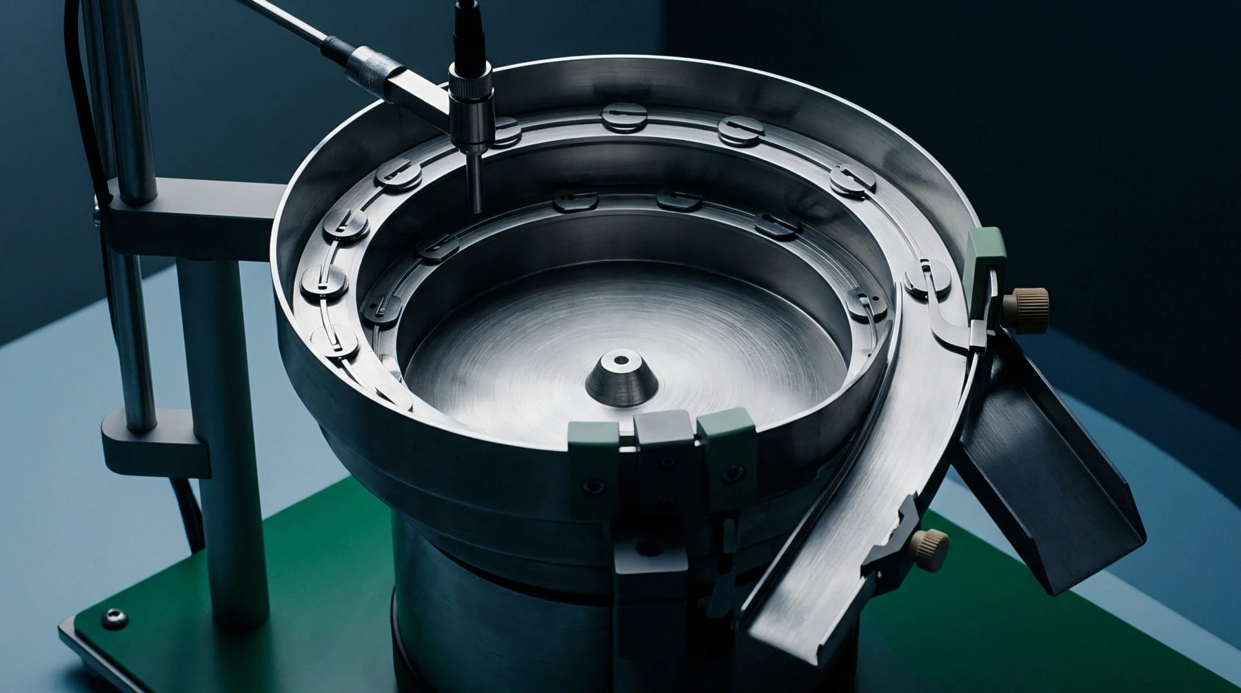
Destructive microsectioning validates barrel copper thickness and layer registration against IPC-6012 criteria to prevent uninspected PCB assembly field failures.
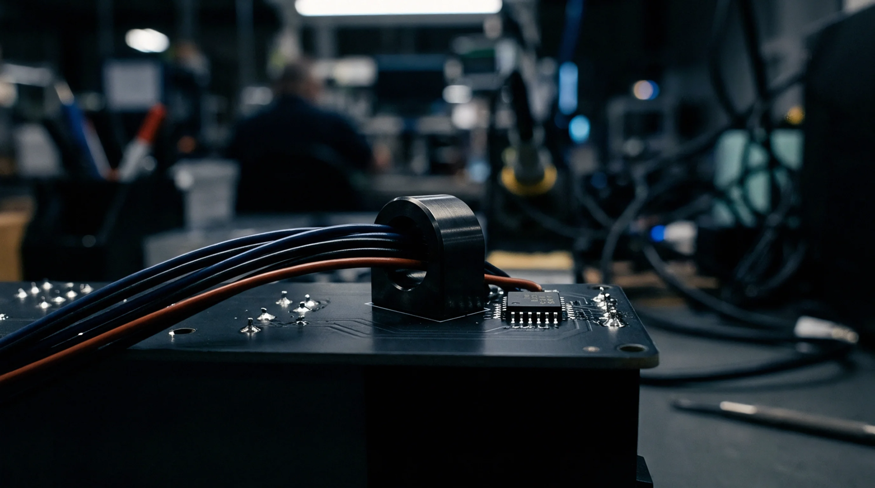
IPC-4552B guardbanding demands shifting ENIG acceptance limits inward by expanded XRF uncertainty, requiring polycapillary optics on fine microvias to prevent false lot rejections.

Controlled dropjetting prevents corrosive flux residue from reaching adjacent SMT lands, maintaining surface insulation resistance without post-solder washing.

Statistical registration stacking balances drill wander and core movement, defining annular ring limits that protect Class 3 reliability and production yield.

Controlled ENIG gold thickness between 0.04 and 0.07 micrometers prevents brittle intermetallic fractures and black pad failure on fine-pitch BGA assemblies.
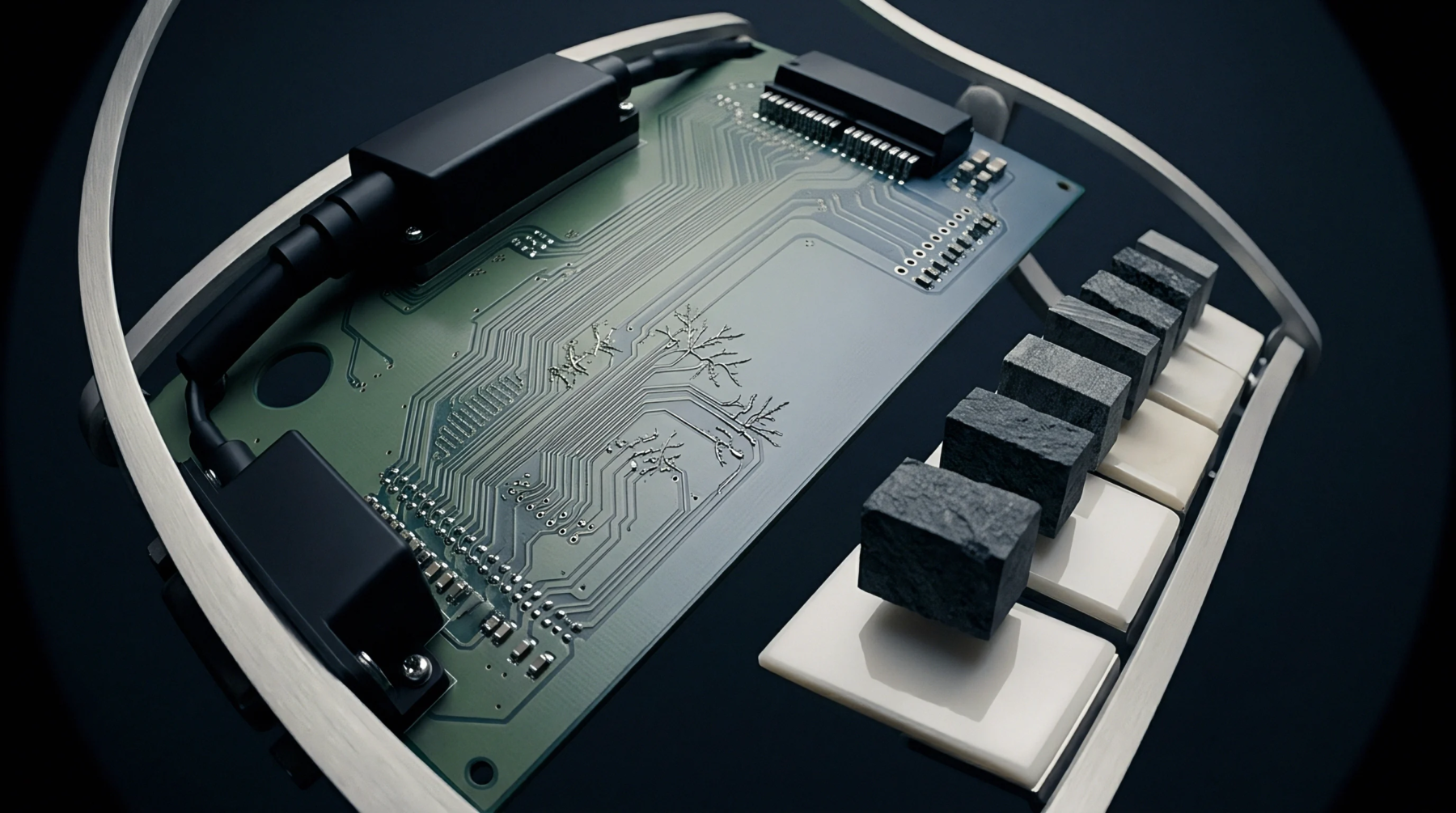
Fine pitch assemblies demand strict surface finish thickness controls to prevent solder bridging, black pad corrosion, and brittle intermetallic joint failures.

Titanium anodization degradation in lead-free waves accelerates TiSn2 dissolution, requiring thickness monitoring to prevent alloy bath contamination.

High aspect ratio multilayers resist cyclic thermal stress when barrel wall ductility exceeds eighteen percent and copper plating thickness remains uniform.

Subtier die shrinks raise thermal impedance, causing standard stress screens to under-heat junctions and pass latent defects directly into finished goods.
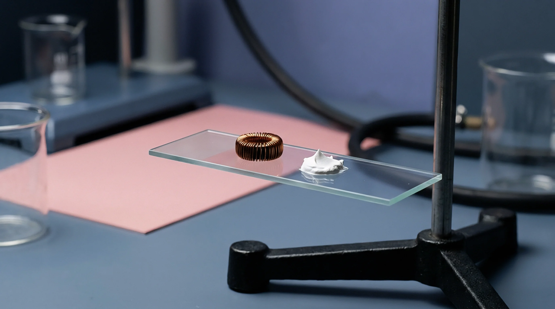
Dynamic high-tin solder waves strip titanium oxide passivity via halide attack and erosion, requiring scheduled thermal re-passivation every 500 operating hours.
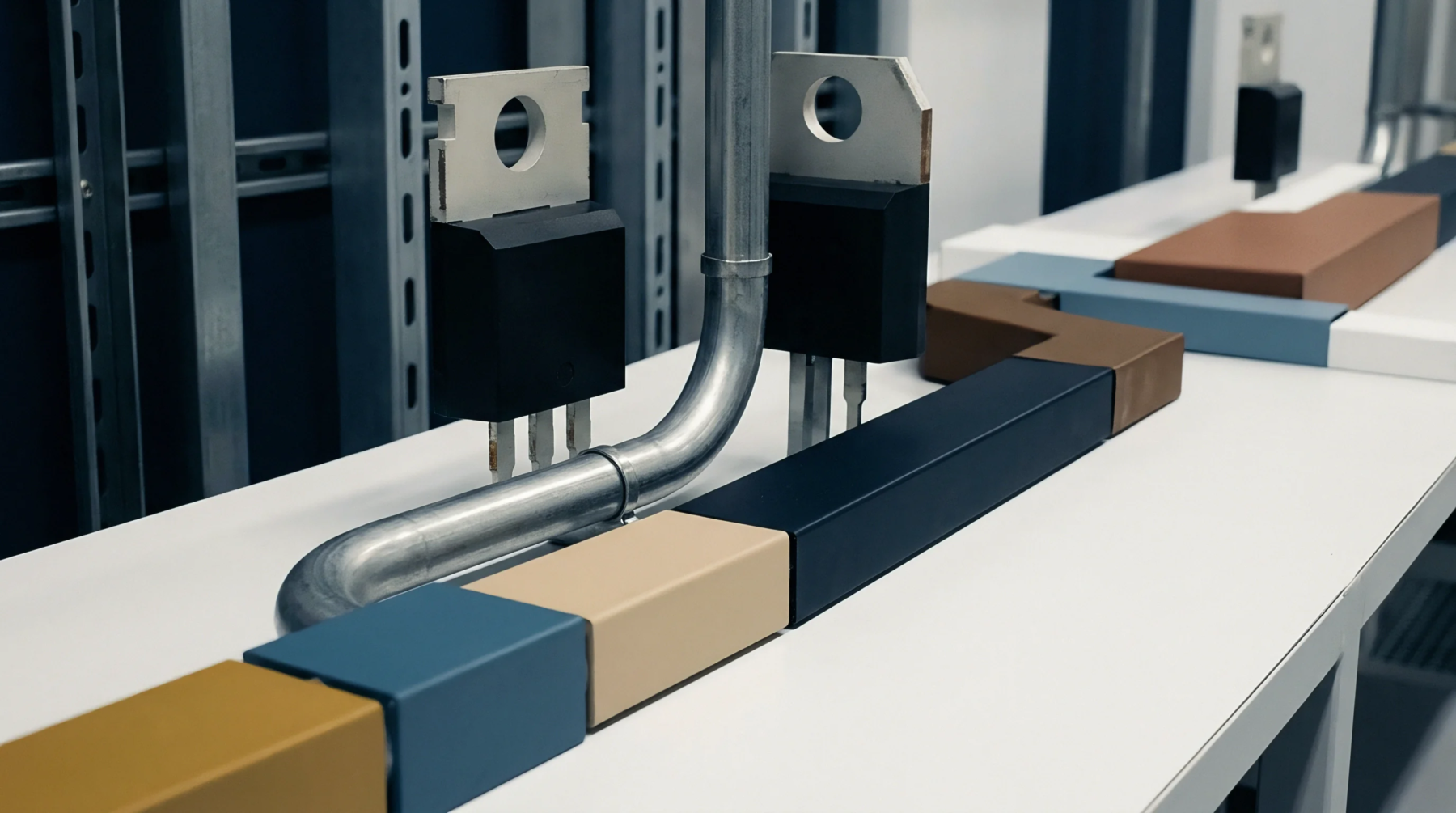
Plating thickness compliance demands precise coupon microsectioning to verify barrel copper, knee integrity, and innerlayer bonds against IPC standards.
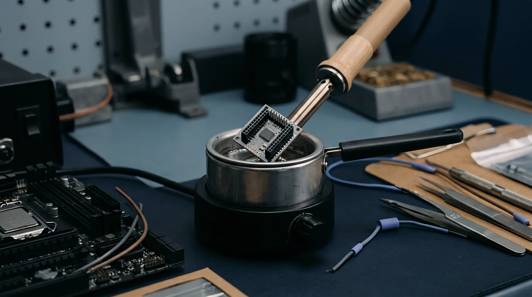
Titanium insert degradation in lead-free soldering drives thread shear and liquid tin dissolution, mitigated by PVD nitriding and controlled torque.

IPC-6012 Class 3 procurement requires mandatory microsection verification per panel, enforcing 25 um average barrel copper and zero hole plating voids.

Parametric sensitivity matrix analysis maps sub-tier component variations to circuit margins, enabling precise guardband testing and enforcing change compliance.

Predictive finite element modeling counters non-affine lamination distortion, securing Class 3 registration and high yields across large substrate formats.
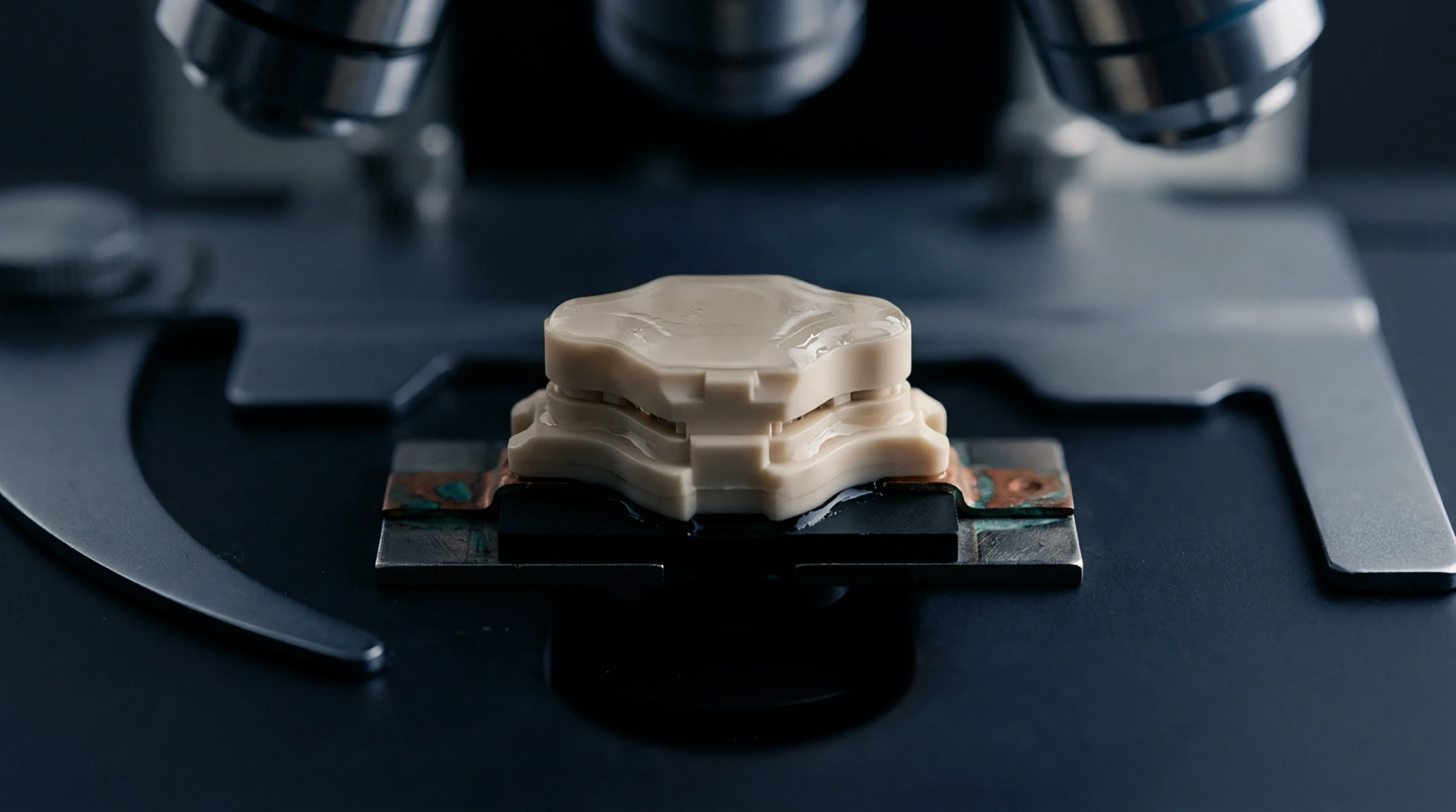
Dynamic platen displacement mapping isolates thermal bowing across press openings to halt position-dependent dielectric variance and layer registration loss.
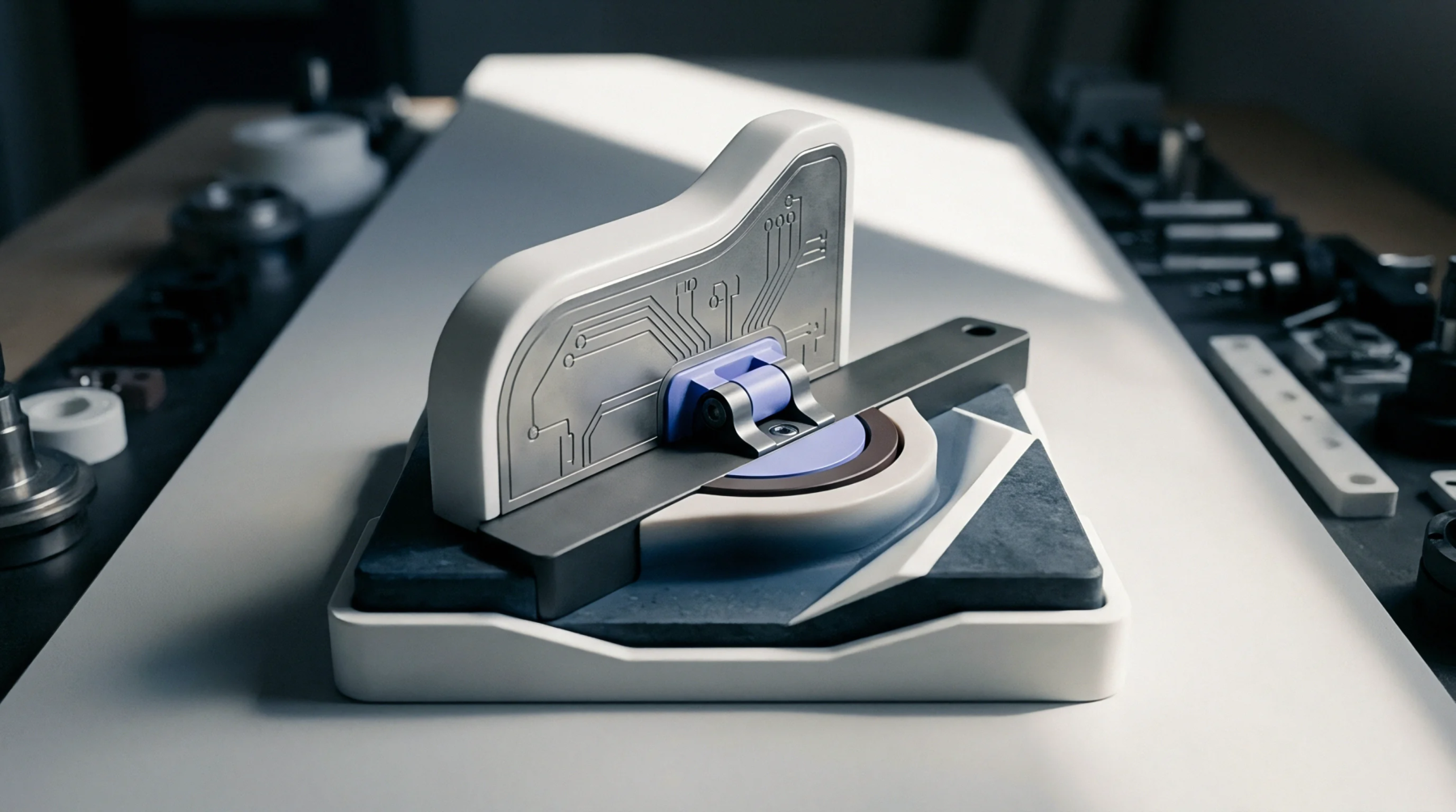
Aperture wall clearances above 1.5mm prevent composite pallets from chilling through-hole barrels below liquidus during nitrogen-shrouded wave immersion.

Inner layer artwork compensation scales CAD vectors dynamically to counteract predictable laminate core press shrinkage and chemical lateral etch undercut.

Nodal test point density below sixty percent demands boundary scan vector verification to prevent catastrophic subtier printed assembly defect escapes.

Correlate Kelvin DC coupon resistance with SEM area integration using a 0.92 geometric factor to resolve flash-etch conductor disputes and allocate scrap costs.
Expertise is a utility, not a secret. sentiention™ publishes its working knowledge as open reference: intelligence layer covering the materials it sources, the markets it enters, and the reference that serves both.